Miniaturisation with embedded component packaging (ECP®)
Embedded component packaging (ECP®) technology uses the space of a multilayer printed circuit board as efficiently as possible. Components can only be attached to the top or bottom of conventional printed circuit boards, but at AT&S we use ECP® to place microcontrollers, resistors and other elements of a circuit within the PCB, too. Using this third level allows us to accommodate many more functions within a smaller space. As they are thinner and more compact, ECP® circuit boards also allow the heat generated in electronic systems to be dissipated more efficiently.

ECP® is a key driver of miniaturisation in fields such as medical technology and consumer electronics. The technology allows thinner and smaller devices to be built without compromising on performance.
Benefits of embedded component packaging (ECP®)
- Highly reliable due to optimal protection of the integrated components and good heat dissipation.
- Thin form factors allow residual heat to be dissipated very efficiently – hugely important in many power electronics control applications.
- The unparalleled degree of miniaturisation allows printed circuit boards to be created in new and smaller shapes.
- Miniaturising the systems keeps signal paths short and losses to a minimum.
Lasers ensure the utmost accuracy
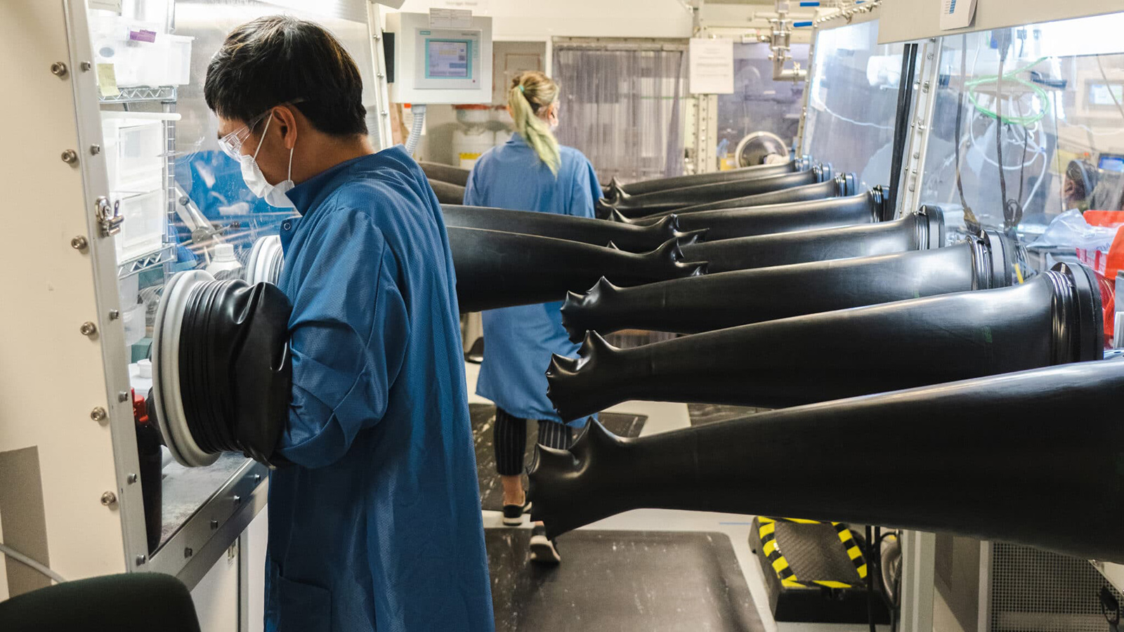
To place an electronic component inside a printed circuit board, we remove targeted areas of material from its inner layers using state-of-the-art laser production systems. The layers are then pressed together to eliminate any remaining space in the cavities, while the embedded components are firmly enclosed and well protected. The connections are then created using laser technology.
ECP® in action
With ECP®, designers of electronic systems enjoy newfound scope for their projects, as they can now position components not only on the surfaces of a circuit board, but also inside.
This allows hearing aids and other medical devices to be miniaturised without affecting the performance of the systems. This is radical miniaturisation for radical new design ideas.
Thin tablets and small hearing aids

ECP® makes it possible for manufacturers of tablets and medical implants to create thinner and smaller devices that still deliver maximum performance. For instance, hearing aids can now be made with very small dimensions, ensuring maximum wearing comfort without compromising on performance.
Efficient power supply
ECP® also plays an important role in the power supply to data centres that facilitate video streaming online. As connections within miniaturised ECP® circuit boards are short, the power supply can be regulated very efficiently and with practically no losses. Such applications can also be found in laptops and smartphone chargers that can charge batteries faster and guarantee optimal runtime.
Want to find out more about the most compact printed circuit boards in the world?
Our printed circuit boards with ECP® technology are the culmination of years of development work in miniaturisation. By “burying” components within a circuit board, we create a third functional level: valuable space is now also available for components inside the circuit board, instead of just on the top and bottom. This allows such a board to fulfill many more functions than a conventional board of the same size. Our ECP® printed circuit boards are used in various high-tech applications, from medical technology to consumer electronics.
Would you like to find out more?
Discover more about the most compact printed circuit boards in the world, serving the global medical, power electronics, data management, industrial, aerospace and communication sectors for more than 10 years.
Download our whitepaper to uncover the capabilities of our Embedding Component Packaging technology and applications.
Contact

If you would like to learn more about our exciting products, technologies and solutions, our experts are always happy to help.
You may also be interested in these topics

Together with globally renowned optical module manufacturers, find out how AT&S is empowering high-speed Optical Module PCB manufacturing to address the increasing demand.
For a long time, rechargeable batteries were just the necessary evil to operate electronic devices. Thanks to the switch from combustion engines to e-cars, the development of new battery technologies has become sexy: Developers are on the hunt for the triad of ultra-fast charging times, long-range and lower production costs.