Thermally enhanced printed circuit boards
Optimum thermal management protects electronics
Modern electronic systems have less and less space, while complexity is increasing constantly. This can cause issues for circuits that generate a lot of heat. At AT&S we offer thermally enhanced PCBs for such applications. These allow heat to dissipate efficiently to protect the electronic circuits and components from overheating. Our various options for managing waste heat can be used as standalone solutions or in combination.
Product benefits at a glance
- Allows components that generate a lot of heat to be directly integrated into the printed circuit board.
- Heat sources at specific points are optimally cooled, while heat flows effectively from the top to the bottom of the printed circuit board.
Self-driving cars and lighting
High heat loads can occur in systems like laser sensors for self-driving cars, the power electronics of electric cars, or in headlights in certain vehicles. Modern lighting concepts based on LED lamps and devices powered by rechargeable batteries also require electronic circuits that can dissipate heat as effectively as possible.
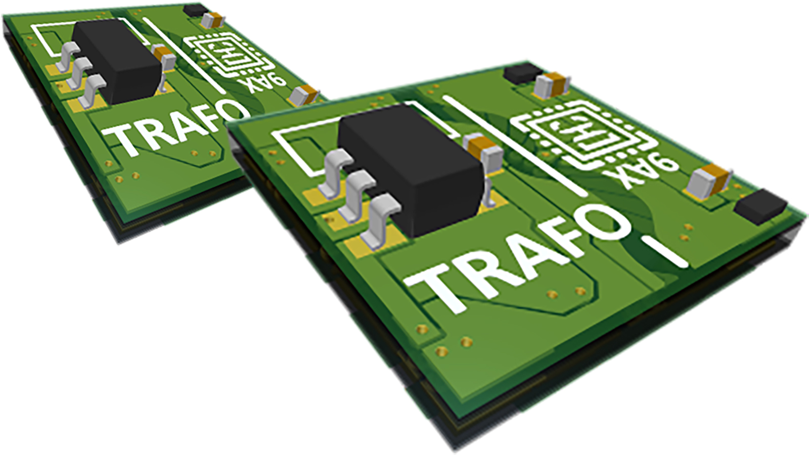
As part of an EU research project, AT&S is developing the next generation of miniaturized inductors that can be integrated into multi-layer printed circuit boards. This makes it possible to implement the smallest voltage converters or ultra-thin, wireless charging devices, which have several advantages compared to the technology currently available.
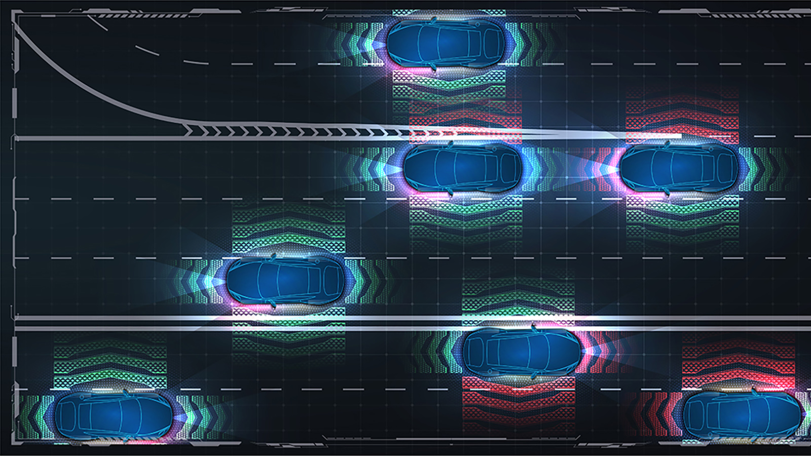
For vehicles to operate as autonomously as possible in the future they must meet completely new requirements in data processing and sensor technology. Cutting edge technology by AT&S enables high-resolution scanning of the surroundings as well as processing and transferring the data volume incurred.
Four out of ten new bicycles are e-bikes, with a steep upward trend putting high demands on development. E-mobility has long become part of everyday life. With leading-edge innovations, AT&S contributes to increasing the efficiency of electric drive systems.
Heat dissipation for any application
Thermal vias
Through-connections that do not use copper to conduct electricity, or do not use it solely for that purpose but instead include it primarily for heat dissipation, are a standard method of heat management on printed circuit boards. Sophisticated technology allows these connections, known as “thermal vias”, to be packed together more densely, which can significantly improve heat management of electronic systems on printed circuit boards. Thermal vias can also be combined with other technologies, such as inlays for thermally enhanced printed circuit boards.
Inlays
At AT&S we have the expertise to integrate copper parts into printed circuit boards. These metal inlays allow heat to be absorbed at specific points and released again on the underside of the PCB. They are used in applications such as car headlights, laser sensors for self-driving cars and charging electronics for electric vehicles. They allow components that generate a lot of heat to be integrated directly into the circuit board, which further reduces the space required for LED elements and other applications. This gives car manufacturers and other producers of electronic systems more leeway in designing components.
Insulated metal substrates
Another way of dealing with the build-up of heat is to give the entire printed circuit board a metal base. To do this, a base material is combined with a 1.6 mm layer of aluminum or copper that absorbs the heat and then releases it across the largest possible surface area into the surrounding air or to a heat sink fitted to the underside of the PCB.
The core feature of this base material is the electrically insulating dielectric layer, which prevents unwanted electrical contact between the signal-conducting layer and the heat-absorbing metal layer. The dielectric layer is also highly thermally conductive due to the mix of different, mostly ceramic components. Such systems are used in LED lighting systems and power electronics for controlling battery charging.
Technical data
| Product Characteristics | Specifications |
|---|---|
| Layer Count | Aluminium: Single sided Copper: Single sided to 3 layers |
| PCB Thickness | Aluminium: 1 or 1.6 mm Copper: 1 mm |
| Thermal Conductivity | 0.4 – 5 W/mK |
| Min. Line | Spacing: 150/150 µm |
| Smallest Drill | 1.50 mm |
| Product Characteristics | Specifications |
|---|---|
| Layer Count | 4 or 6 layers |
| Thermal Conductivity of Copper Inlay | 360 – 390 W/mK |
| Inlay Thickness | 0.8 or 1 mm |
| Inlay Dimensions | min. 10 x 10 mm |
| Spacing between Inlays | min. 6 mm |
Want to find out more about AT&S for the automotive sector?
AT&S has a long tradition in the automotive industry. Our printed circuit boards are included in headlights, power electronics and entertainment systems, and are helping drive advancements in manufacturing.
Find out more about our solutions for the automotive industry, see here:
You may also be interested in these topics
Electronic components for autonomous vehicles in the mining industry must meet the highest standards in terms of robustness and failure safety. This is the only way they can presist in the challenging environment of a mine.
As part of the "IPCEI on Microelectronics and Communication Technologies" funding project, the European Union is supporting research institutions and industrial partners in the development of technology that will enable a sustainable yet powerful data infrastructure for the continent. AT&S is involved in the project as a manufacturer of highly efficient substrates for the next generation of microchips. New research and production capacities in Leoben will play a decisive role in the modernization of the European microelectronics industry.
From ChatGPT to EU regulation of artificial intelligence: 2023 has ushered in a new phase of digitalization that will transform our society.


