HDI Circuit boards
A breakthrough with HDI
In printed circuit board manufacturing, “HDI” stands for “high density interconnect”. HDI printed circuit boards have played an important role in the history of AT&S; indeed, they marked the beginning of the company’s rise to become the market leader in the manufacture of high-end PCBs. The high circuit density and small structures enable tiny form factors for devices like mobile phones and digital cameras, and make the process of controlling engines and other complex systems efficient.
Product benefits at a glance
- Higher circuit density enables a high degree of miniaturisation.
- Short and fast connections mean high data rates.
- The compact design keeps line lengths and losses to a minimum.
- HDI technology can be combined with other AT&S processes to create highly adaptable printed circuit boards.
- Eco-friendly materials without halogens can be used during production.
High density for modern electronics
In 1997, the first HDI multilayer printed circuit boards were developed for mass production for the mobile phone market, which was in its infancy. The multilayer printed circuit boards made it possible to embed complex circuits within a small space. The high degree of miniaturisation, the short and rapid signal paths and the resulting reduction in energy consumption were exactly what mobile phone manufacturers needed at the time.
To achieve this, laser systems were used for the first time to create precise holes in the printed circuit board. This established the new practice of working with sequential build-up layers layers (SBU), which are pressed layer by layer into a compact circuit board. Ever since then, HDI printed circuit boards have been indispensable in the electronics industry ever since.
HDI printed circuit boards are used in satellite communications, driving assistance systems, consumer electronics, aircraft, engine controls, digital cameras, smartphones and medical devices.


Laser takes the place of drills

The booming electronics industry has already developed a whole array of new products featuring Anylayer technology. Powerful smartphones, wireless headphones, miniaturised video cameras, smart glasses and tiny sensors for industry and medical technology could not have been achieved by any other means. If maximum performance is required in a tiny space, HDI Anylayer printed circuit boards provide the solution.
Anylayer technology is the next step in the evolution of HDI printed circuit boards. All of the connections between the individual layers of the printed circuit board are created in the form of laser-drilled holes, known as microvias. This saves space and improves signal conductivity. There are almost no constraints on the way that individual layers of a printed circuit board can be interconnected using this method. Electronics manufacturers can create even more complex circuits with HDI Anylayer printed circuit boards, while miniaturising their devices to an even greater degree at the same time.

HDI as a springboard for progress
HDI printed circuit boards have triggered a leap forward in miniaturisation in electronics. At AT&S, they form the basis for many advanced technologies that allow even smaller systems. Without them, we wouldn’t be using compact cameras, smartphones, drones and other consumer electronics today. See our blog for an overview of some fascinating potential applications.
Bendable even with densely packed components
The booming electronics industry has already developed a whole array of new products featuring Anylayer technology. Powerful smartphones, wireless headphones, miniaturised video cameras, smart glasses and tiny sensors for industry and medical technology could not have been achieved by any other means.
Contact

If you would like to learn more about our exciting products, technologies and solutions, our experts are always happy to help.
You may also be interested in these topics

From weddings to beach vacations, drones are currently the most exciting tool in the equipment for many amateur filmmakers and photographers. Connection technology from AT&S ensures excellent communication between the multitude of components, from GPS and sensors to high-resolution cameras on board.
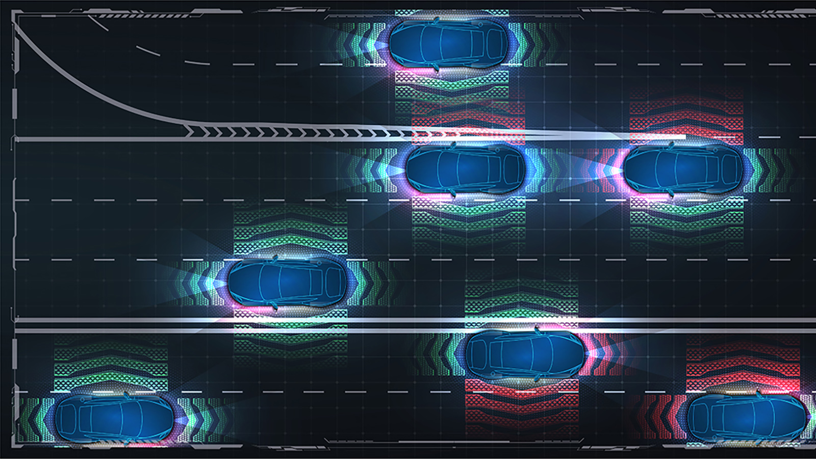
For vehicles to operate as autonomously as possible in the future they must meet completely new requirements in data processing and sensor technology. Cutting edge technology by AT&S enables high-resolution scanning of the surroundings as well as processing and transferring the data volume incurred.

As part of the "IPCEI on Microelectronics and Communication Technologies" funding project, the European Union is supporting research institutions and industrial partners in the development of technology that will enable a sustainable yet powerful data infrastructure for the continent. AT&S is involved in the project as a manufacturer of highly efficient substrates for the next generation of microchips. New research and production capacities in Leoben will play a decisive role in the modernization of the European microelectronics industry.