Advanced Interconnect
Solution Services
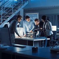
The AT&S “Advanced Interconnect Solution Services” (AISS) department offers a broad range of services beyond conventional PCB manufacturing. Its main areas of responsibility include supporting customers in designing PCBs and IC substrates and assisting them in virtual product development. Together with our partners for assembly, packaging and testing, we greatly simplify the development process for new systems and the optimisation of existing products for our customers.
Our services are organised in five different areas:
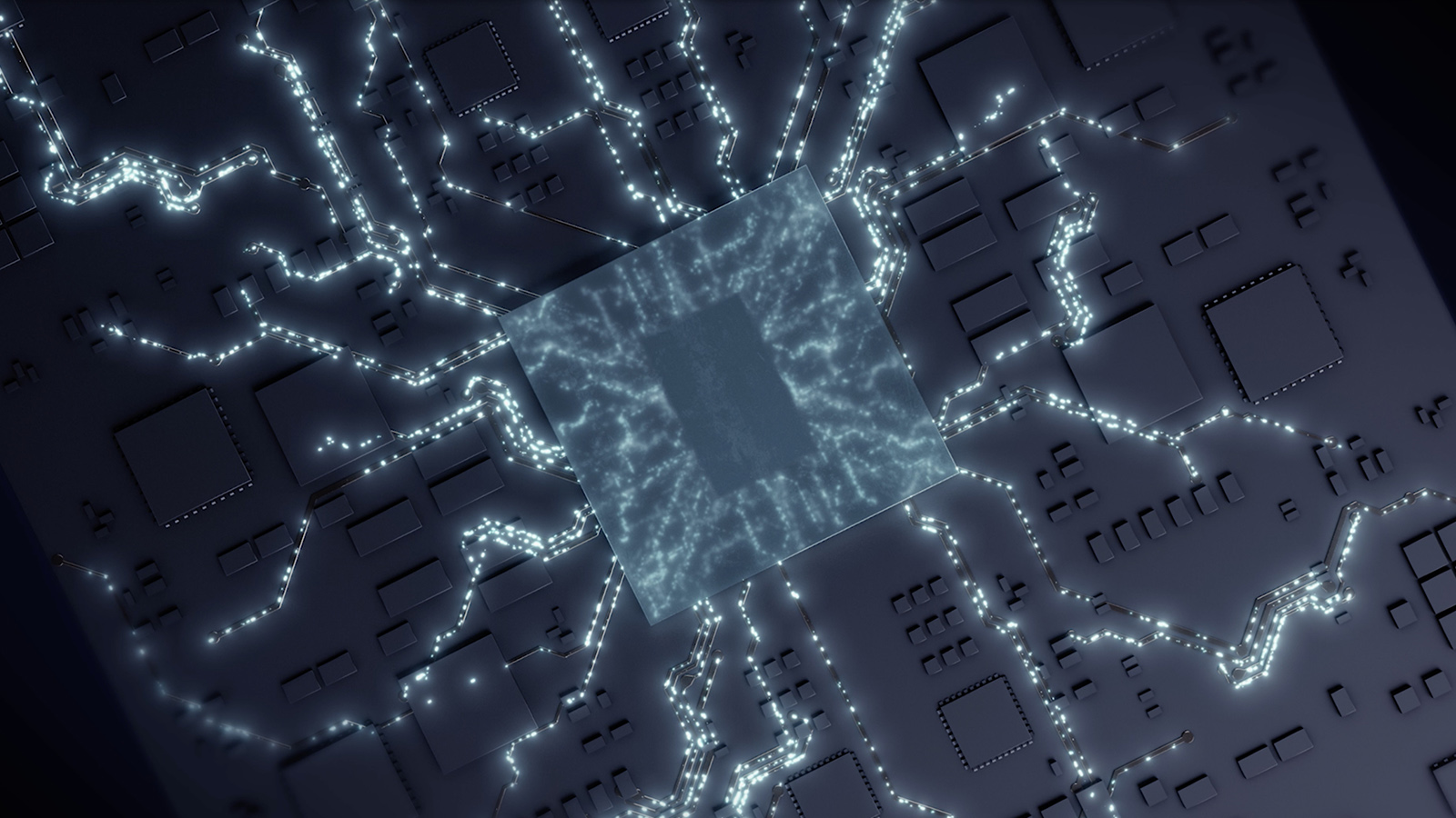
The PPS Team (Product & Process Simulation) offers simulations at the highest technical level for a variety of different areas. Virtual tests are conducted to determine how PCBs react to warping or twisting, how thermal load is distributed and how reliable a system is under realistic conditions.
The HDC Team supports our customers in complex technical tasks such as designing new circuits.
Our RF Team dedicates itself to the latest concepts in RF design, for example the integration of RF structures of passive filters and antennas. They also carry out complex impedance and loss simulations in order to improve the signal line.
Our Product Development Team (PDS) provides customers with assembly services carried out by proven partners. In addition, the team coordinates AISS services ranging from design, simulations, RF optimisation and assembly to PCBA testing conducted by our FTD Team (Functional Test Development). This ensures fast and cost-efficient product and module development for our customers.
Our service department AISS supports customers at every step in their product development phase, from design to simulation-based improvements and testing.

Design
We support our customers in developing technical concepts and carry out PCB layout tasks for any desired circuit. We translate product requirements into customised design. Thanks to AT&S’s extensive capabilities in the area of substrate and PCB production, we can guarantee fast and cost-efficient conversion into finished products.
We have extensive knowledge in component embedding (ECP®) and PCB optimisation and work with leading development tools and industry standards. This allows us to meet a broad range of customer requirements. AISS enables customers to convert layout data into a data set suitable for manufacture within a very short period of time.

Simulation

AISS acts as a service centre for simulation services within the company. AT&S can thus access comprehensive know-how and state-of-the-art characterisation methods for mechanical and electrical properties of base materials. This knowledge, for example of directional mechanical properties within a PCB or substrate material, allows precise modelling and consequently also improved simulations. Twisting or warpage problems or even problems in the reflow process can therefore be identified and mitigated at an early stage. Customers benefit from the fact that production rejects can be significantly reduced. Moreover, the complex models allow conclusions on the reliability of vias and solder connections of a PCBA, which ultimately leads to a more reliable product.
Product Development Services
On request, we also support our customers throughout the complete development cycle of a product, from the design to the manufacture of the product. In this process, we collaborate closely with our proven partners. AISS coordinates the design, simulation, assembly and tests in order to guarantee smooth cooperation with our clients. As a result, our customers can fully concentrate on new innovations, while we assist them in optimally implementing their ideas.

Contact
We are here for you!
If you would like to learn more about our exciting products, technologies and solutions, our experts are always happy to help.
You may also be interested in these topics
Technological upheavals such as self-driving cars and the increasing importance of data centers are driving the demand for high-performance computer chips to unimagined heights. AT&S benefits from this development and assumes responsibility for the development of the future vision of the semiconductor industry.
The manufacture of printed circuit boards will be included in the curriculum of Indian universities.
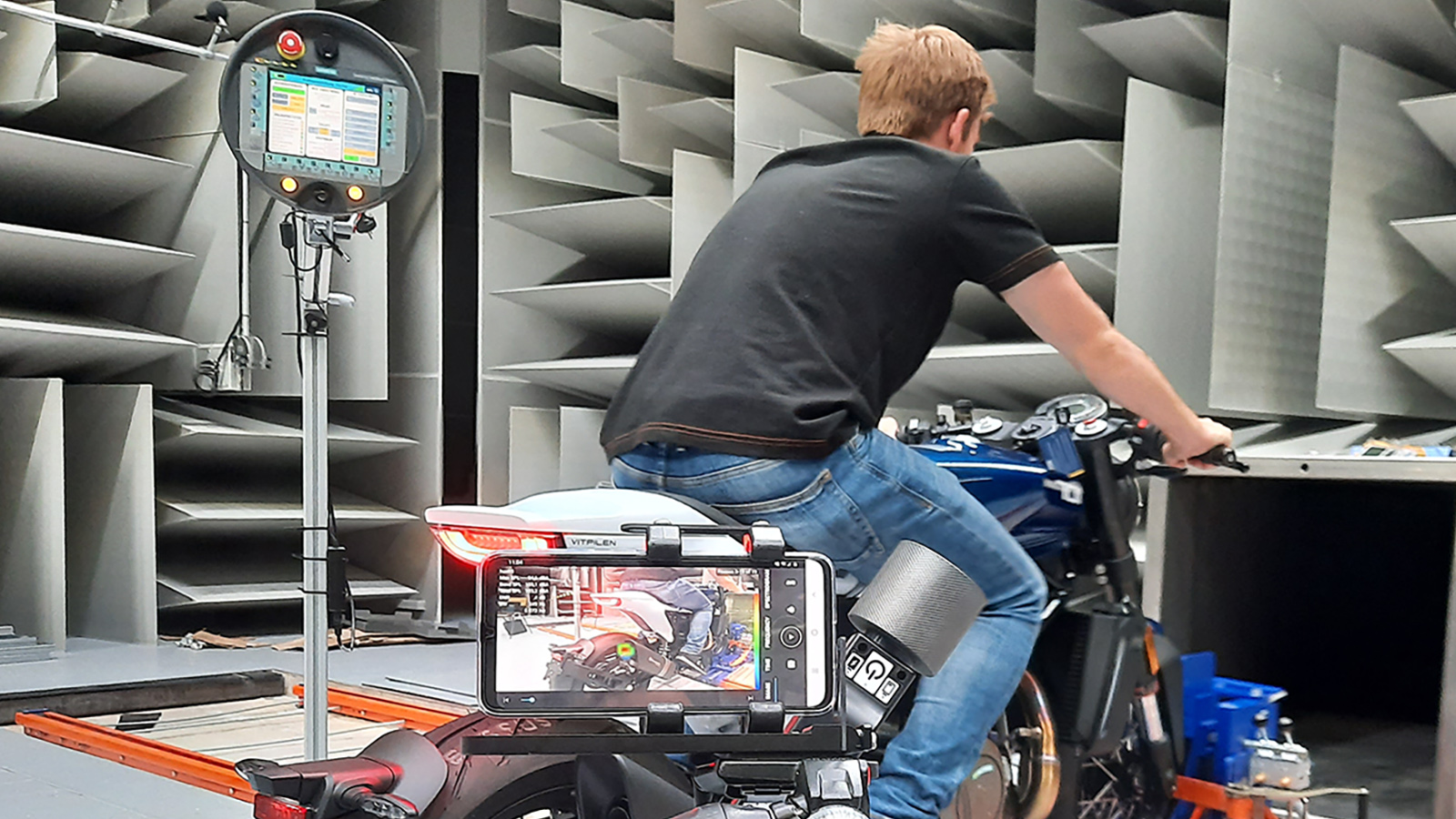
The Upper Austrian start-up SevenBel has developed a method to make noise sources visible, enabling engineers to prevent undesirable noise in buildings or devices. AT&S high-tech printed circuit boards are part of the sensor units making this possible.