AT&S Empowers High-Speed Optical Module PCB Manufacturing
Together with globally renowned optical module manufacturers, find out how AT&S is empowering high-speed Optical Module PCB manufacturing to address the increasing demand.
These new applications will further increase the market demand for data center computing power. The advent of large-scale AI systems not only brings about the need for server accelerator cards but also requires higher data transmission speeds and lower latency. This can be achieved through high-speed optical conversion devices in data centers. Manufacturers are continuously introducing better modules with faster speeds and higher capacities to meet market demands for data centers, undersea cables, base stations, and other communication infrastructure. According to YOLE’s prediction, the global market size for optical modules will increase from $10.5 billion in 2021 to $24.7 billion in 2027, with a compound annual growth rate of 15%.
As optical modules evolve from 400Gbps to 800Gbps and then to 1.6Tbps, they drive the development of appropriate optical module Printed Circuit Board (PCB) technology towards higher speed, greater density, and better heat dissipation. AT&S has been collaborating with well-known optical module manufacturers worldwide for many years. Through these partnerships, AT&S was able to achieve mass production of 100G to 400G optical module PCBs, and the 800G optical module PCB products have already passed customer verification. Furthermore, AT&S is also conducting preliminary research on 1.6T optical modules and Co-Packaged Optics (CPO) with customers.
AT&S, established in 1987, is one of the global leading manufacturers of high-tech PCBs and IC substrates. Its customers include top global manufacturers in the fields of smartphones, automotive electronics, chips, servers, base stations, and other high-end consumer electronics. AT&S’s worldwide manufacturing sites are industry benchmarks with their state of the art technologies, advanced equipment, and unrivaled know-how in advanced manufacturing. AT&S’s expertise in optical module PCB manufacturing technology mainly covers the following areas:
- High-end Substrates-like PCB (SLP) technology: Through the modified semi-additive process (mSAP), it can achieve substrate level line spacing, effectively improving layout density and achieving miniaturization. In addition, the mSAP process improves graphical accuracy and reduces impedance fluctuations. The process allows the copper lines to have almost perfect vertical sidewalls, thereby reducing losses caused by the skin effect. When mSAP is applied to the outer layers, it is also possible to connect bare dies to reduce signal losses, making mSAP especially suitable for applications at 800G and higher frequencies[1].

mSAP technology
- 2.5D technology: Facilitates the embedding of a wide range of components in PCBs, reduces the thickness of the overall product. Additionally, the close proximity of the components reduces the length of the gold wires, which provides higher signal bandwidth and minimal losses.
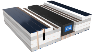
2.5D technology
- Laser Trench process: By increasing the number of electrical connections between adjacent power and ground layers, this process reduces thermal resistance and improves heat dissipation in optical modules.
- Low-roughness brown oxide process: This process utilizes special techniques and chemicals to reduce the roughness of copper surfaces while maintaining bond strength, thereby reducing conductor losses caused by the skin effect.
- Support for arbitrary-level HDI (High-Density Interconnect) and the stacking of laser blind vias with mechanical buried vias (FV2) meets the requirements of different optical module architectures.

High-Density Interconnect
- Embedded Component Packaging (ECP®) process: It supports the embedding of active components or capacitors. With this solution, capacitors are embedded in two or more layers of core boards, reducing the path lengths between ICs, decoupling capacitors and improving power filtering effects.
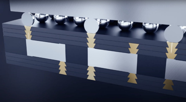
Embedded Component Packaging ECP®
- Strong R&D team and simulation capabilities to provide simulation analysis for thermal performance, warpage, stress, high-speed signal loss, and electromagnetic compatibility (EMC), which help to address the main concerns of optical module customers. AT&S’s simulation process covers both pre-simulation and post-simulation for the design phase, as well as failure analysis during the engineering phase. Moreover, AT&S has improved on industry-standard simulation software, developing proprietary intellectual property, secondary development algorithms, and a comprehensive materials database for internal use. Validating the results with sophisticated testing methods allows the simulations to become even more accurate and closer to real-world conditions. AT&S’s simulation capabilities provide accurate virtual analyses and predictions at different stages of a customers’ product development, helping them to optimize designs, improve product performance, reduce costs, and cut time to market.
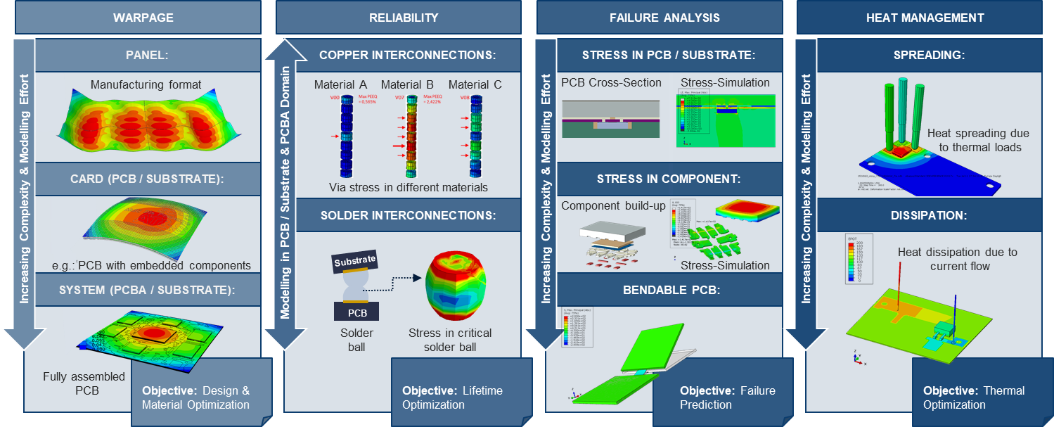
AISS simulation
For more information about AT&S products or technologies, please contact Richard Chenoweth:
Email: sales@ats.net
Phone: +1 408 573 7287
[1] “Co-packaged Optics for Datacenter 2023” by Yole Intelligence
Share post: