Multilayer printed circuit boards
A many-layered success story
Multilayer printed circuit boards are AT&S’s core business and form the basis for most technologies used for further miniaturizing electronic circuits and systems. At the dawn of modern electronics, printed circuit boards were simple resin-bonded paper with circuits printed on one side. But technology soon developed in response to increasing demands for integrating and miniaturizing electronics.
Product benefits at a glance
- Multilayer printed circuit boards ensure short and fast signalling pathways.
- The layered structure allows for complex circuits.
- The compact design enables further miniaturisation of circuits and devices.
Miniaturisation drives innovation
Modern circuits on printed circuit boards have a structure comprising multiple functional layers, so they can make the most of their short signalling pathways and accommodate complex systems within tiny spaces. Many applications would simply be unfeasible without the possibilities that this opens up for more complicated circuits. The rapid miniaturisation that we have seen in consumer electronics, mobile communications and smart devices over the past few years would be almost inconceivable without the invention of multilayer printed circuit boards.

MRI scanners and satellite communications
Today, AT&S can produce printed circuit boards with four to 78 layers, which can be adapted to almost all system manufacturer requirements. Multilayer printed circuit boards have contributed to technological progress in a wide range of areas, including satellite communications, information processing, magnetic resonance imaging (MRI), control technology in the automotive industry and flight control. Multilayer designs also play an important role in networked devices to make homes and workplaces smarter, so they will remain an integral feature of microelectronic systems in high-tech applications.


Contact

If you would like to learn more about our exciting products, technologies and solutions, our experts are always happy to help.
You may also be interested in these topics
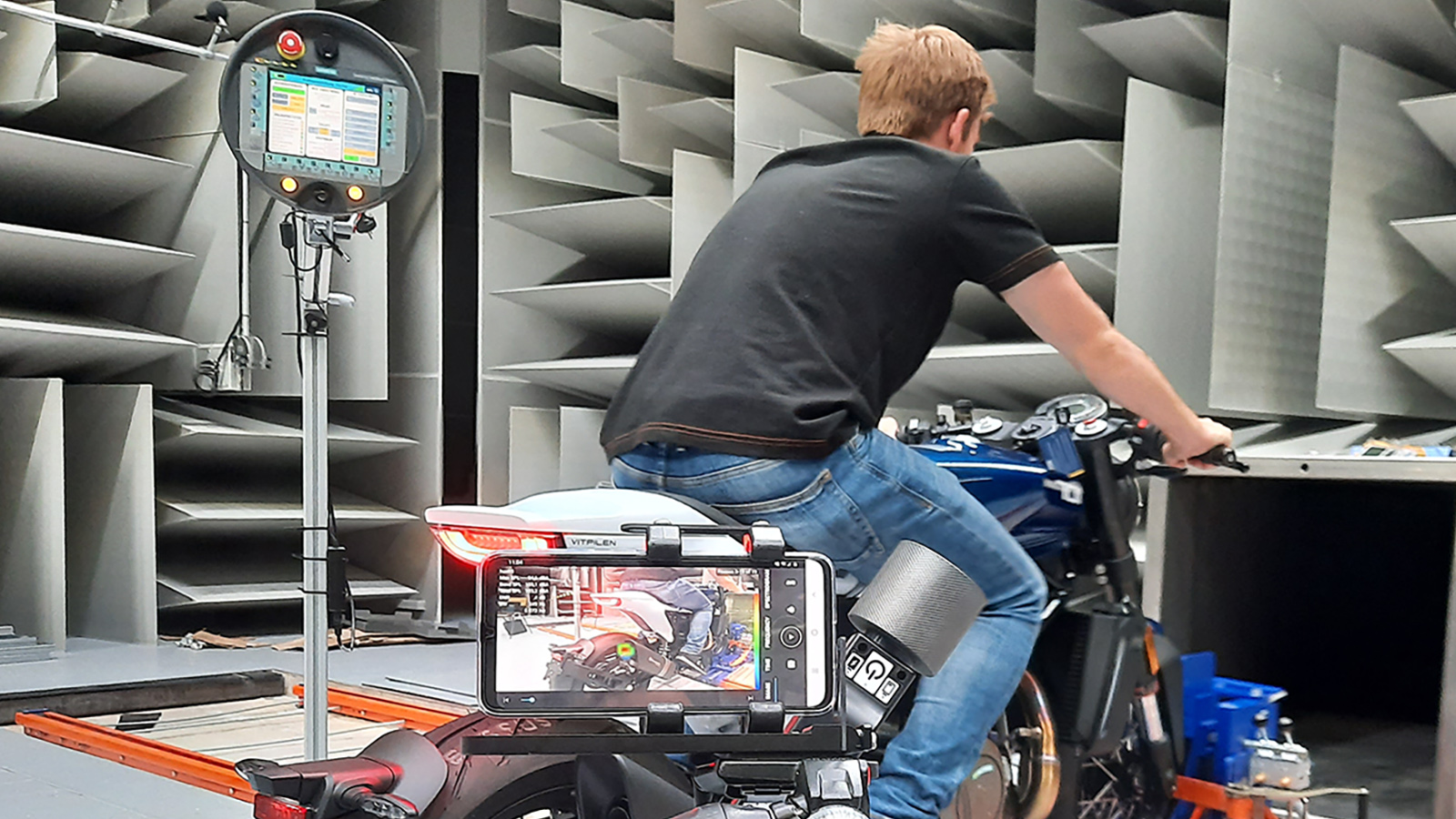
The Upper Austrian start-up SevenBel has developed a method to make noise sources visible, enabling engineers to prevent undesirable noise in buildings or devices. AT&S high-tech printed circuit boards are part of the sensor units making this possible.
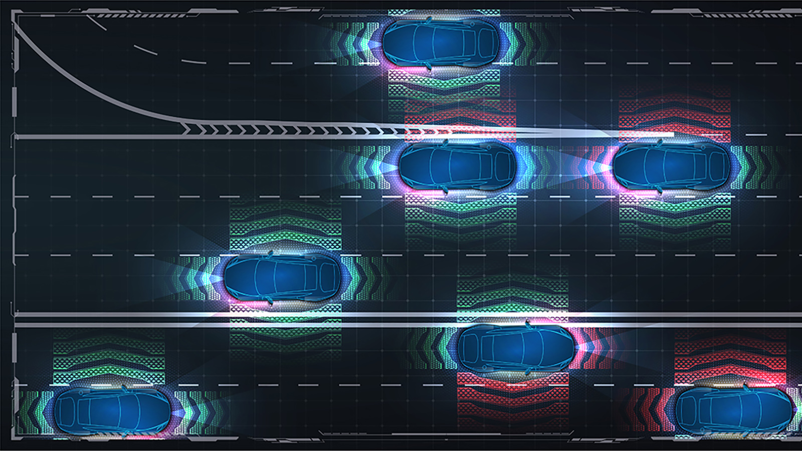
For vehicles to operate as autonomously as possible in the future they must meet completely new requirements in data processing and sensor technology. Cutting edge technology by AT&S enables high-resolution scanning of the surroundings as well as processing and transferring the data volume incurred.

As part of the "IPCEI on Microelectronics and Communication Technologies" funding project, the European Union is supporting research institutions and industrial partners in the development of technology that will enable a sustainable yet powerful data infrastructure for the continent. AT&S is involved in the project as a manufacturer of highly efficient substrates for the next generation of microchips. New research and production capacities in Leoben will play a decisive role in the modernization of the European microelectronics industry.