


Sustainable innovation for AT&S and its customers
The electronics industry is characterised by ongoing rapid development and regular technological breakthroughs. AT&S customers are among the market leaders in their respective sectors. They expect our products and processes to meet the very highest standards and be flexible enough to keep up with the rapid pace of innovation in the industry.
Our own focus on R&D means that we are constantly developing our technology to ensure that customers can always see their ideas take shape as effectively as possible. Since the very founding of AT&S, we have proven that bold investment in R&D pays off. We value sustainable concepts highly and use the latest technologies to reduce the environmental footprint of our own group and our partner companies.

Whether in technology, business processes or implementing environmental improvements, innovation is the driving force behind AT&S, from the initial idea right through to execution. We’re playing a key role in shaping an interconnected future.
Hannes Voraberger, Director of R&D
Faster, greener, better connected
We strive to actively shape the technology of tomorrow and offer our customers creative solutions to their technical problems. After all, that’s the only way of staying one step ahead of the competition and continuing to play a crucial role in the microelectronic revolution, and play a significant role in solving the major challenges facing our society. At the same time, powerful electronic systems are driving the digitisation and decarbonisation of the economy by opening the way for cost-effective, flexible control of a wide variety of systems: wind power plants, for example, can only be used efficiently if they are controlled intelligently. The same goes for the microchips in powerful computers, servers and mobile devices.
AT&S technology powers processors and enables communication between microchips and the other components that a computer needs.
Our printed circuit boards and substrates not only ensure rapid data processing, but also make a real contribution to keeping energy consumption as low as possible through further miniaturisation. By making the utmost demands of ourselves and our suppliers in terms of environmental responsibility, AT&S always ensures that our technological advances do not come at the expense of the environment. We take a holistic approach to the world of tomorrow. See our comprehensive concept for sustainable production, which is constantly being expanded to include more environmentally friendly materials and energy-saving infrastructure. We are proactive in ensuring that the future not only brings progress, but also remains worth living in.
Sustainable.
As a high-tech company, we harness our expertise to keep our demand for raw materials and energy as low as possible while protecting the environment. We recycle materials, manage our water and energy consumption efficiently and will have decarbonised all of our sites by 2030. For more information about our efforts for a world worth living in, see here:
Research as a driving force
In order to maintain our status as leaders in technology and environmental responsibility, we invest 10% of our revenue in research and development of new products and processes. At present, this amounts to around €120 million per year. Our locations in Austria benefit hugely from this investment and have already seen a whole host of state-of-the-art technologies made ready for series production.

AT&S holds more than 700 patents for the manufacture of high-tech printed circuit boards and IC substrates. These innovations are responsible for a significant part of our revenue, with 21% currently derived from products and technologies that have been brought onto the market in the past three years, following a development phase of several years.

We support research inside and outside the company
Besides having a world-class in-house research department, AT&S also uses its products to drive progress in a number of different fields. For instance, our substrates are used in supercomputers and have become indispensable in many branches of science. To find out more, see here:
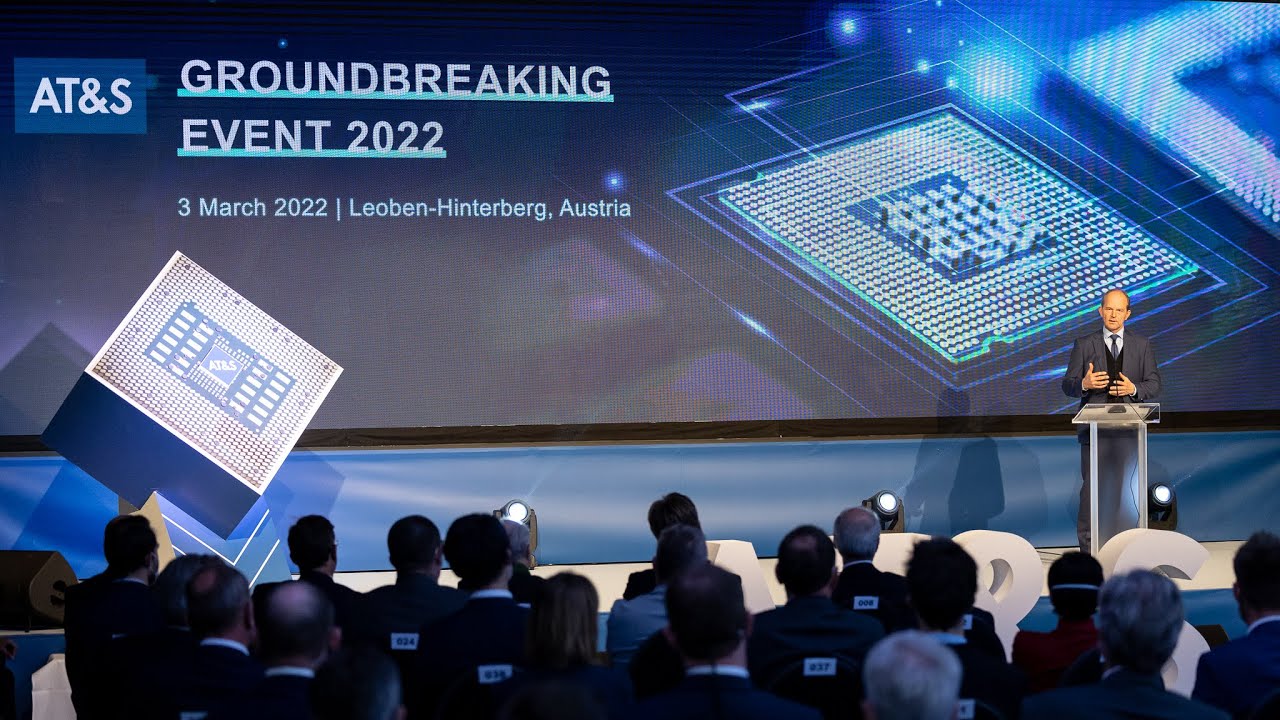
New R&D Centre: high tech in Austria and the rest of Europe

Over the next few years, AT&S is set to invest €500 million in a new research centre in Leoben that will employ 700 new people.
A new research and development centre with an attached production facility will be built at the AT&S headquarters in Leoben by 2025. Some €500 million will be invested in the construction of a new building that offers over 10,000m2 for research and production. A total of 700 new jobs will be created at the site.
The new building marks the group’s commitment to ongoing technological development and to the Leoben site itself. It will see the creation of many new products and ideas, which will continue to ensure a bright future for AT&S. The new research department will also attract expertise in the production of IC substrates to Leoben, so that Austria will once again be able to draw upon major talent in high-tech electronics and the semiconductor industry.
This is a lighthouse project for Europe, as it will be the only substrate production facility on the continent. Substrates will become even more prominent when Leoben undergoes expansion.


Data, data, data
At the epicentre of the boom in the electronics industry lies the data revolution, which has utterly transformed industry and everyday life over recent years. Increasing amounts of data are being recorded, stored and analysed in order to handle processes as efficiently as possible and enable people to access a wide variety of online services. These developments require data processing systems that consume as little energy as possible and transmit signals efficiently, while still allowing for a high degree of complexity. Whether in the automotive industry, medical technology or semiconductor production, designers and manufacturers of microelectronic systems can meet these requirements with printed circuit boards and substrates from AT&S.
Through ongoing technological development, we ensure that our circuit boards are in the top division for efficiency in terms of energy consumption and signal transmission.
We develop and optimise our products in collaboration with our customers, and now in a fully digital environment.
This not only simplifies improvements, but also the implementation of measures that reduce our environmental footprint. We share this approach with our suppliers and business partners, so together we can help shape priorities for the entire production ecosystem. We strive for the lowest consumption of resources with the highest possible miniaturisation of microelectronic systems to ensure efficient data processing and a high-speed, energy-saving signal line.


We always have the right answer
Creative technical approaches and innovation have always been the foundation for the growth and business success of AT&S. Thanks to our concentrated focus on research and development, we always come up with the right solution for technical challenges, in collaboration with our customers.
Institutes & industry partners
We stay at the forefront of technology in our industry by working together with some of the world’s most renowned research institutes, including the Fraunhofer Institute in Germany, Graz University of Technology, the Montanuniversität Leoben, Silicon Austria Labs, the Indian Institute of Technology and Virginia Tech University in the USA. Through a combination of high investment and excellent research partners, we are consolidating our technological leadership and helping to initiate future breakthroughs in the electronics industry.


Promoting research: AT&S projects and collaborations
As an innovative high-tech company, AT&S is an important part of the research landscape in Austria and Europe as a whole. The high quality of our development work means that we can benefit from prestigious funding programmes and cooperate with an array of internationally renowned partners. For more information, see here:
![]() Optimised Operation and Design of Industrial Energy Systems
Optimised Operation and Design of Industrial Energy Systems
The overarching aim of DigitalEnergyTwin is to give the industry a methodology and software tool that provides precise support for optimising the operation and design of the industrial energy system.
Applying the digital twin methodology facilitates the development, validation and streamlining of highly detailed energy system modelling for selected energy-related processes and renewable power supply technologies.
Interdisciplinary knowledge transfer in electronic-based systems (EBS) to boost players in the value chain
The Inno-EBS (electronic-based systems) qualification programme focuses on teaching state-of-the-art cross-cutting skills in hardware, embedded software and systems.
The programme is aimed at target groups from these areas and professionals in innovation management in general. It deals with the most pertinent EBS-related concerns of companies through four target group-specific tracks.
![]()
Challenging environments require tolerant smart systems for the IoT and AI
The CHARM project deals with solutions for the application of ECS (electronics, components and systems) technologies in harsh industrial environments. Demonstrator applications from six different industrial sectors (mining, paper mills, the grinding industry, manufacturing of solar cells, digital printing, and the maintenance and decommissioning of nuclear power plants) will be developed as part of the project.
CHARM will open up new business areas and value chains within Europe while also promoting production in Europe by creating new opportunities for digitalisation and contacts with the ECS community, giving rise to digital solutions.
![]() Highly EFFICIENT and reliable electric drivetrains based on modular, intelligent and highly integrated wide band-gap power electronics modules
Highly EFFICIENT and reliable electric drivetrains based on modular, intelligent and highly integrated wide band-gap power electronics modules
This project focuses on the development of state-of-the-art, integrated and reliable wide band-gap (WBG) technologies, including highly energy-efficient and reliable power electronics for electric vehicles and charging infrastructure.
This will drive smart mobility, which will have a significant impact at all levels throughout the value chain. The HiEFFICIENT partners have set themselves ambitious goals for achieving greater acceptance and harnessing the maximum benefit when using WBG semiconductors.
![]()
Intelligent Reliability 4.0
The Intelligent Reliability 4.0 (iRel4.0) project seeks the overarching goal of significantly improving the reliability of electronic systems throughout the entire value chain (from development and production through to application, all the way to the end of the component’s life).
Innovative test methods and the extended implementation of sensor-based system control will make it possible to identify risk components and systems, and to implement new models of maintenance.
Electronic components and systems provide solutions for the major challenges that society will face in future, especially in terms of mobility (autonomous driving, e-mobility), power generation (wind energy) and digitalised industry.
![]()
Research for GaN technologies, devices, packages and applications to address the challenges of the future GaN roadmap
The UltimateGaN project has set itself the aim of significantly improving the carbon footprint of digitalisation. It will address this through efficiency gains using future generations of gallium nitride (GaN) technologies and packages for the electronics industry in Europe.
The GaN devices created as part of UltimateGaN will open the way for a wide range of innovative, energy-efficient applications, with the far-reaching aim of supporting digitalisation and thereby consolidating Europe’s leading position in the field of electronic components and systems.
![]()
D-band radio 5G network technology
The DRAGON project will overcome the limitations of current E-band wireless backhaul solutions by using the D-band (130–174.8 GHz)1 radio spectrum to achieve a suitable high-capacity radio solution with a small form factor. This is essential for it to be deployed on a massive scale, enabling the speed of optical systems to be carried across to backhaul systems at low cost. DRAGON offers great prospects for new semiconductor, antenna and packaging technologies and the resulting hardware devices to come onto the market and create new economic opportunities.
![]()
Important Project of Common European Interest on Microelectronics
The Important Project of Common European Intereston Microelectronics (IPCEI Microelectronics) endeavours to strengthen the European microelectronics industry with the aim of promoting microelectronics technology throughout the EU. The IPCEI on Microelectronics was approved by the European Commission in December 2018 and will run until March 2024.
The IPCEI on Microelectronics includes projects with a focus on research and development, along with the first industrial deployment (FID) in the following five areas of technology:
- energy-efficient chips
- power semiconductors
- sensors
- advanced optical devices and
- composites.
Some 32 companies and research and development institutions from Austria, France, Germany, Italy and the UK are involved in the IPCEI on Microelectronics partnership.
And it’s not just the members of the consortium that benefit from the IPCEI. Lessons learned as part of the project will benefit organisations across Europe, creating positive spillover effects throughout the entire semiconductor value chain and in other areas.
AT&S – part of the IPCEI on Microelectronics
As part of the IPCEI on Microelectronics, AT&S is leapfrogging existing packaging technologies in carefully selected areas and focusing on implementing next-generation packaging technology in Austria. It achieves this by pooling and combining the three main areas of excellence at AT&S:
- High-end printed circuit boards
- Substrate technology
- Component integration
Our four working packages:
- Functional cores for power-efficient substrates and packages
- Brand new packaging concepts for high-speed and high-frequency electronics
- Miniaturisation for new test and reference boards and other applications
- Advanced production and testing capacities
IPCEI spillover tasks handled by AT&S include:
- Collaboration with industry & researchAs part of the IPCEI, AT&S supports and boosts development activities throughout the value chain across Europe, in conjunction with universities and research and technology organisations (RTOs). These efforts will have a positive impact on transmission for Europe.
- Supporting training and talent
AT&S will promote the involvement of universities in the STEM sector
Unique System enables AT&S and customers to dive into the world of semiconductor processes
As part of its R&D line, AT&S has decided to purchase a physical thin film system “Clusterline 600” from Evatec. This new technology is used for the development of next-generation IC substrates, novel embedding concepts, heterogeneous integration, advanced packaging and FO-PLP (Fan-Out – Panel Level Packaging).
Contact

We are here for you!
If you would like to learn more about our exciting products, technologies and solutions, our experts are always happy to help.
You may also be interested in these topics

As part of the "IPCEI on Microelectronics and Communication Technologies" funding project, the European Union is supporting research institutions and industrial partners in the development of technology that will enable a sustainable yet powerful data infrastructure for the continent. AT&S is involved in the project as a manufacturer of highly efficient substrates for the next generation of microchips. New research and production capacities in Leoben will play a decisive role in the modernization of the European microelectronics industry.

From ChatGPT to EU regulation of artificial intelligence: 2023 has ushered in a new phase of digitalization that will transform our society.

The resurrection of the Beatles for new songs and Sean Connery as the best James Bond ever in new films? This will soon no longer be a problem for the brave new world of AI.