ECP® (embedded component packaging) printed circuit boards
The most compact printed circuit boards in the world
Our printed circuit boards with ECP® technology are the culmination of years of development work in the field of miniaturisation. By “burying” components within a circuit board, we create a third functional level: valuable space is now also available for components inside the circuit board, instead of just on the top and bottom. This allows such a board to fulfil many more functions than a conventional board of the same size. Our ECP® printed circuit boards are used in high-tech applications ranging from medical technology to consumer electronics.

Product benefits at a glance
- ECP® printed circuit boards enable more compact systems and smaller devices.
- Moving components inside the printed circuit board affords them better protection, while freeing up room on the outer layers.
High precision with laser technology
To place components inside a printed circuit board, we remove targeted areas of material from its inner layers using state-of-the-art laser technology. The components are then placed in the recesses so that no gaps remain. The connections are then created by laser drilling.
AT&S uses the latest laser technology to create the most compact circuit ever to be produced with PCB (printed circuit board) sector tools.
Access systems, implants and tablets
ECP® printed circuit boards are important within diverse areas of the electronics industry. Their thin design makes them ideal for use in ultra-thin smartphones and tablets. Tiny communication modules can also be enclosed in smart pens and other unusual form factors that open up new possibilities in consumer electronics.
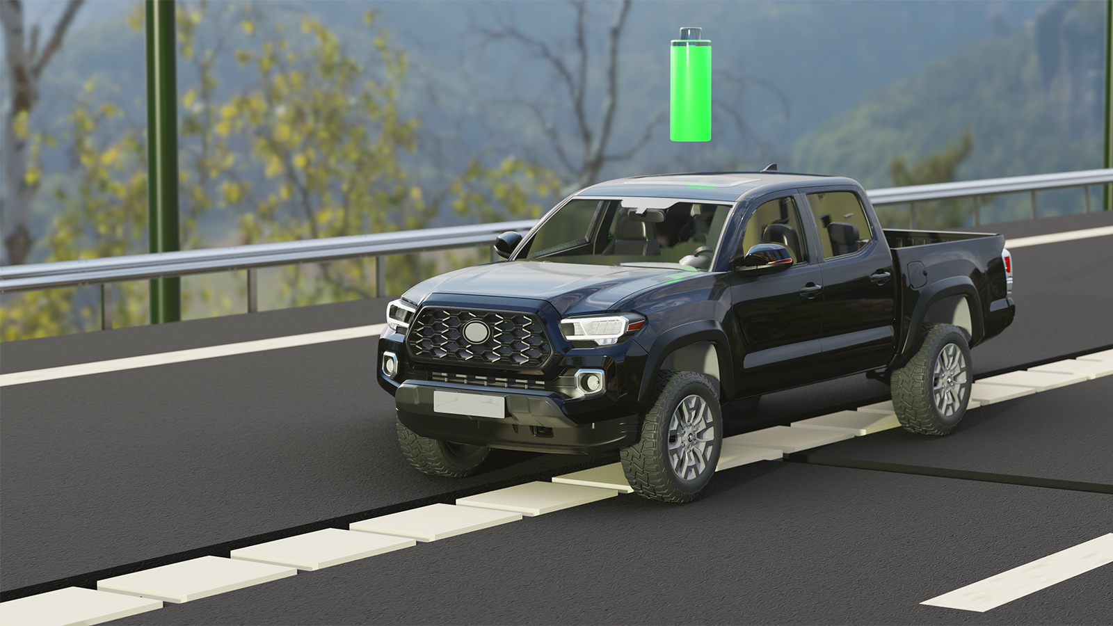
Speaking of smartphones, these small circuit boards enable a larger, longer-lasting battery. Chargers with ECP® technology enable these batteries to charge more quickly. Electronic access controls, data centres, smart factories and medical technology all benefit from the reduced system size and enhanced reliability of these PCBs.


Technical details

| Product Characteristics | Specifications |
|---|---|
| Layer count | 4 to 12 layers |
| Embedded core layer count | 2 or 4 layers |
| Copper nominal thickness | RCC: 12 to 22 µm PP: 12 to 35 µm |
| Die to package ratio | >35% |
| Component thickness | 60 to 300 µm |
Would you like to find out more?
Discover more about the most compact printed circuit boards in the world, serving the global medical, power electronics, data management, industrial, aerospace and communication sectors for more than 10 years.
Download our whitepaper to uncover the capabilities of our Embedding Component Packaging technology and applications.
Contact

If you would like to learn more about our exciting products, technologies and solutions, our experts are always happy to help.
You may also be interested in these topics
Technological upheavals such as self-driving cars and the increasing importance of data centers are driving the demand for high-performance computer chips to unimagined heights. AT&S benefits from this development and assumes responsibility for the development of the future vision of the semiconductor industry.

As part of the "IPCEI on Microelectronics and Communication Technologies" funding project, the European Union is supporting research institutions and industrial partners in the development of technology that will enable a sustainable yet powerful data infrastructure for the continent. AT&S is involved in the project as a manufacturer of highly efficient substrates for the next generation of microchips. New research and production capacities in Leoben will play a decisive role in the modernization of the European microelectronics industry.