Taking printed circuit boards to a whole new level with 2.5D®
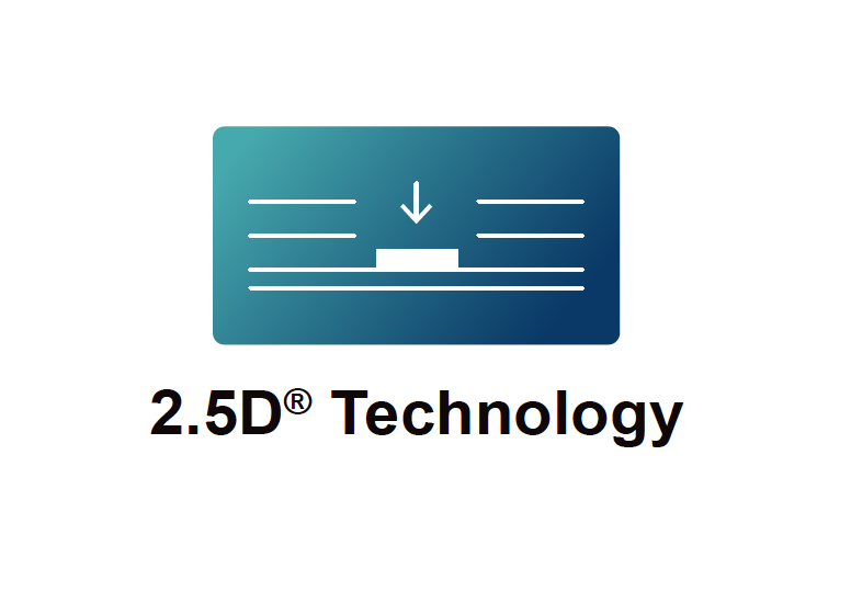
2.5D® technology from AT&S allows the creation of custom recesses in individual layers of multi-layer printed circuit boards. Not only does this technology open the way for lower-lying components, resulting in highly compact PCBs, but it also allows the material in the PCB to be thinned out to such a degree that it becomes flexible and can be bent for installation. This makes 2.5D® a highly versatile development that ushers in completely new PCB designs. 2.5D® can help to get top performance out of SSD hard drives, driver assistance systems and laser sensors.

2.5D® technology gives AT&S the option of removing precise parts of a printed circuit board in order to place components lower down. This makes it possible to manufacture extremely thin PCBs. Removing parts of the middle layers makes the circuit board flexible.
Benefits of 2.5D® technology
- The cavities allow circuits and printed boards to be extremely miniaturised and thin.
- Compared with other technical alternatives, 2.5D® allows designs to be made more flexibly and miniaturised in a cost-effective way.
- The cavities can be positioned and adjusted as required.
Less is more
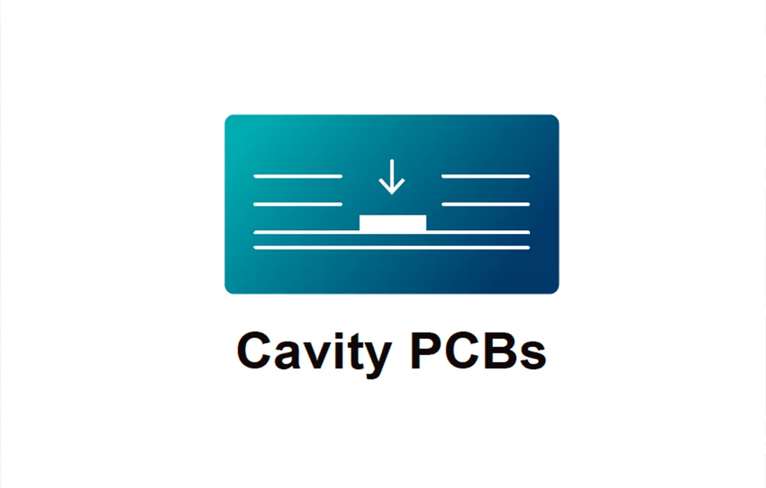
These partial recesses (referred to as “cavities”) can be created in printed circuit boards using 2.5D® technology. Electronic components, no matter how complex, of an electronic circuit can be placed in these cavities on the inner layers of a printed circuit board. “Lowering” components in this manner creates a compact design for electronic circuits, as the volume of a printed circuit board can be used much more efficiently, and thinner systems are created as a result. This is particularly interesting for smartphone manufacturers, for example, who are keen to keep the space on the printed circuit board required for antennae and signal processing as small as possible.
2.5D® technology makes the most of the space available for a circuit.
2.5D® in action


Cavities alter properties
Multiple cavities can be easily integrated into a single printed circuit board. The depth and shape of the recesses can be customised to accommodate each component. Connections for active components that need access to a power supply also can be installed within a cavity. Strategic positioning of cavities and components means that key PCB properties. e.g. heat dissipation and permeability of radio signals for wireless communication, can also be adjusted at low cost. Coating the cavities with metal can also protect them against electromagnetic interference.
2.5D® for bendable PCBs
2.5D® technology can also be used to produce semi-flexible printed circuit boards, which opens up even more options for designers of electronic circuits. So much material is removed from the inner layers of the PCB in this process, that its mechanical properties are altered and it becomes somewhat flexible. This can allow PCBs to be bent 90 or 180 degrees during installation, saving space while keeping the connections between different areas fast and reliable. These semi-flexible PCBs are especially durable and enable extremely compact, highly integrated circuits to be installed.
Best price
2.5D® printed circuit boards can be produced using standard materials, so relatively few process steps are involved in their manufacture. What’s more, fitting components within the cavities often proves more efficient than placing them on the surface or completely embedded within the PCB. For instance, PCBs for driver assistance and camera systems in self-driving cars can be designed to fold or bend during installation, thus keeping the space they require to a minimum. SSD memory devices of the kind used in computer hard drives or USB sticks have a semi-flexible design, which allows them to have a larger surface area with a comparable volume, and thus store more data. 2.5D® technology also allows cavities and semi-flexible areas to be combined within a single PCB.
Want to find out more about consumer electronics solutions from AT&S?
New technologies are always needed to meet the growing demands of the systems required by the ever-improving performance of consumer electronics products and the miniaturisation of electronic devices. Innovative products from AT&S inspire developers to bring out ever smaller and more powerful devices and meet the requirements of the advanced applications of the future.
Contact

If you would like to learn more about our exciting products, technologies and solutions, our experts are always happy to help.
You may also be interested in these topics

Together with globally renowned optical module manufacturers, find out how AT&S is empowering high-speed Optical Module PCB manufacturing to address the increasing demand.

Since the beginning of time, man has produced a product with outstanding reliability: waste. However, what has rotted for thousands of years has grown over our heads since industrialization and consumer society thanks to non-rotting waste.

As part of the "IPCEI on Microelectronics and Communication Technologies" funding project, the European Union is supporting research institutions and industrial partners in the development of technology that will enable a sustainable yet powerful data infrastructure for the continent. AT&S is involved in the project as a manufacturer of highly efficient substrates for the next generation of microchips. New research and production capacities in Leoben will play a decisive role in the modernization of the European microelectronics industry.