Cavity printed circuit boards
Using space more efficiently
The devices and electronic circuits that facilitate the digital side of our day-to-day lives have to perform increasingly complex tasks at breathtaking speed. One of the key areas of potential for the further development of such systems is miniaturisation, in which increasingly complex circuits are packed onto printed circuit boards in ever denser configurations, so that they require less and less space.
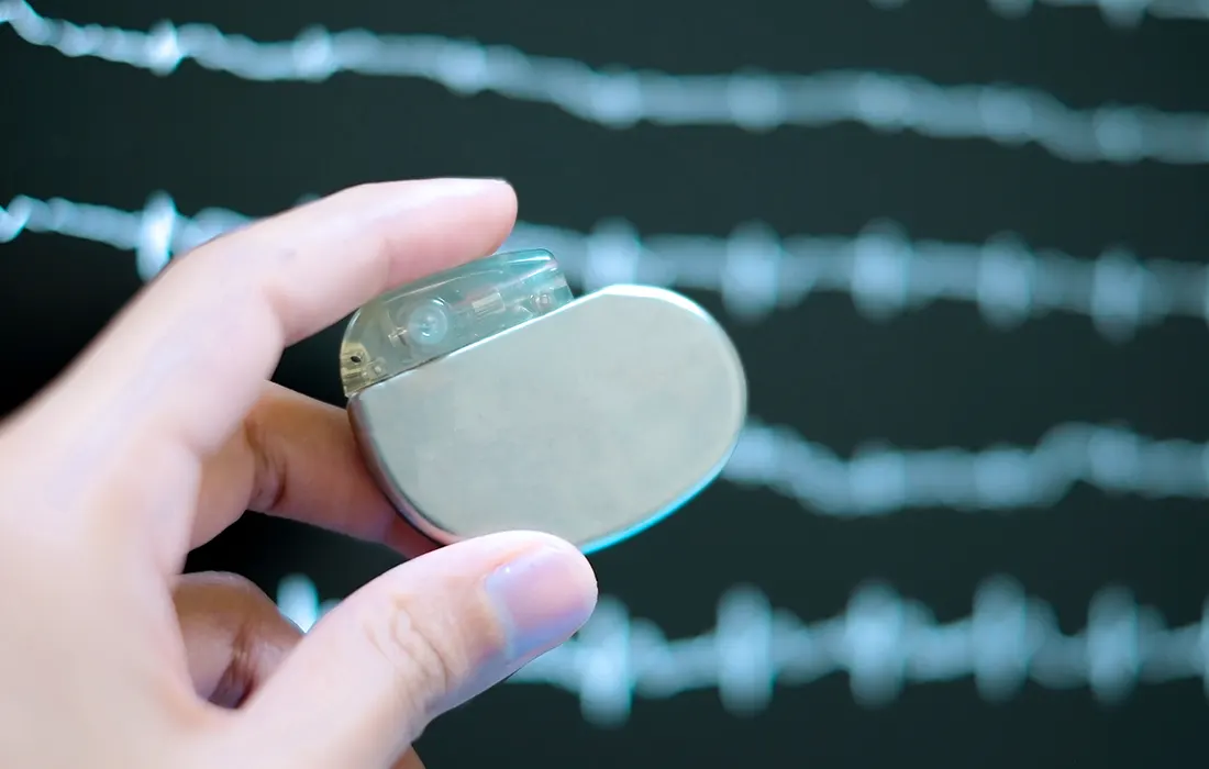
At AT&S, we no longer use just the surface of printed circuit boards for this, but also integrate components into the inner layers. This uses the space of a printed circuit board to the max and makes miniaturised devices such as medical implants and smartphones possible.
Product benefits at a glance
- Cavities allow miniaturisation in PCB technology to go one step further.
- Miniaturisation using cavities is relatively cost-effective compared to other approaches.
- Cavities can be positioned flexibly and easily adapted to the components or new systems.
2.5D – in depth lies strength
As printed circuit boards shrink, the surface area available for traces and components decreases with it. That’s why AT&S is making the most of the space within multilayer circuit boards in its latest high-tech versions. These use 2.5D® technology to remove parts of individual layers of a printed circuit board to create cavities. Components such as resistors, microcontrollers or heat sinks can then be placed in the cavities.
AT&S uses 2.5D technology to make the most of limited space
The cavities are created in a high-precision laser process, and can be designed in any shape. Adjusting the laser beams ensures top-quality surfaces that put as little stress as possible on the processed material. The components housed in the cavities are also well protected inside the circuit board at all times.
Smartphones and driver assistance systems
Removing unneeded circuit board layers reduces losses in high-frequency signals in high-frequency antenna circuit boards, which is particularly important for antenna structures. So printed circuit boards with cavities are very well suited to wireless communication applications such as smartphones and their infrastructure. The waste heat from heat-generating components can also be better managed through the targeted removal of material.


Contact

If you would like to learn more about our exciting products, technologies and solutions, our experts are always happy to help.
You may also be interested in these topics
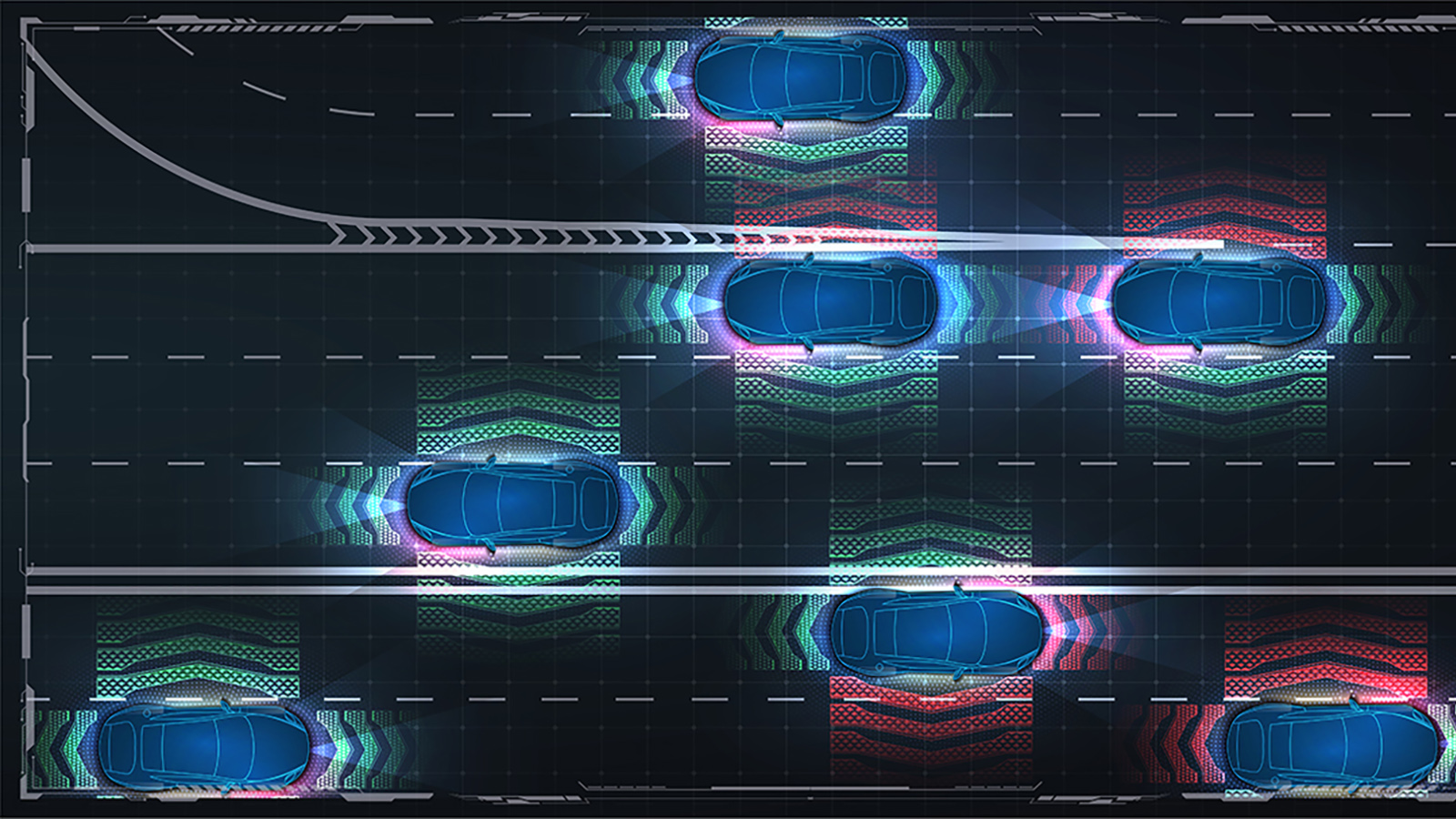
For vehicles to operate as autonomously as possible in the future they must meet completely new requirements in data processing and sensor technology. Cutting edge technology by AT&S enables high-resolution scanning of the surroundings as well as processing and transferring the data volume incurred.

The mSAP technology enables the development of a new geometry for printed circuit boards which provides for faster data connections – an extremely important feature in the information society.

As part of the "IPCEI on Microelectronics and Communication Technologies" funding project, the European Union is supporting research institutions and industrial partners in the development of technology that will enable a sustainable yet powerful data infrastructure for the continent. AT&S is involved in the project as a manufacturer of highly efficient substrates for the next generation of microchips. New research and production capacities in Leoben will play a decisive role in the modernization of the European microelectronics industry.