UTAC and AT&S Collaborate on Turnkey Supply for 3D SiP Solutions with Embedded Chip in Substrate Technology

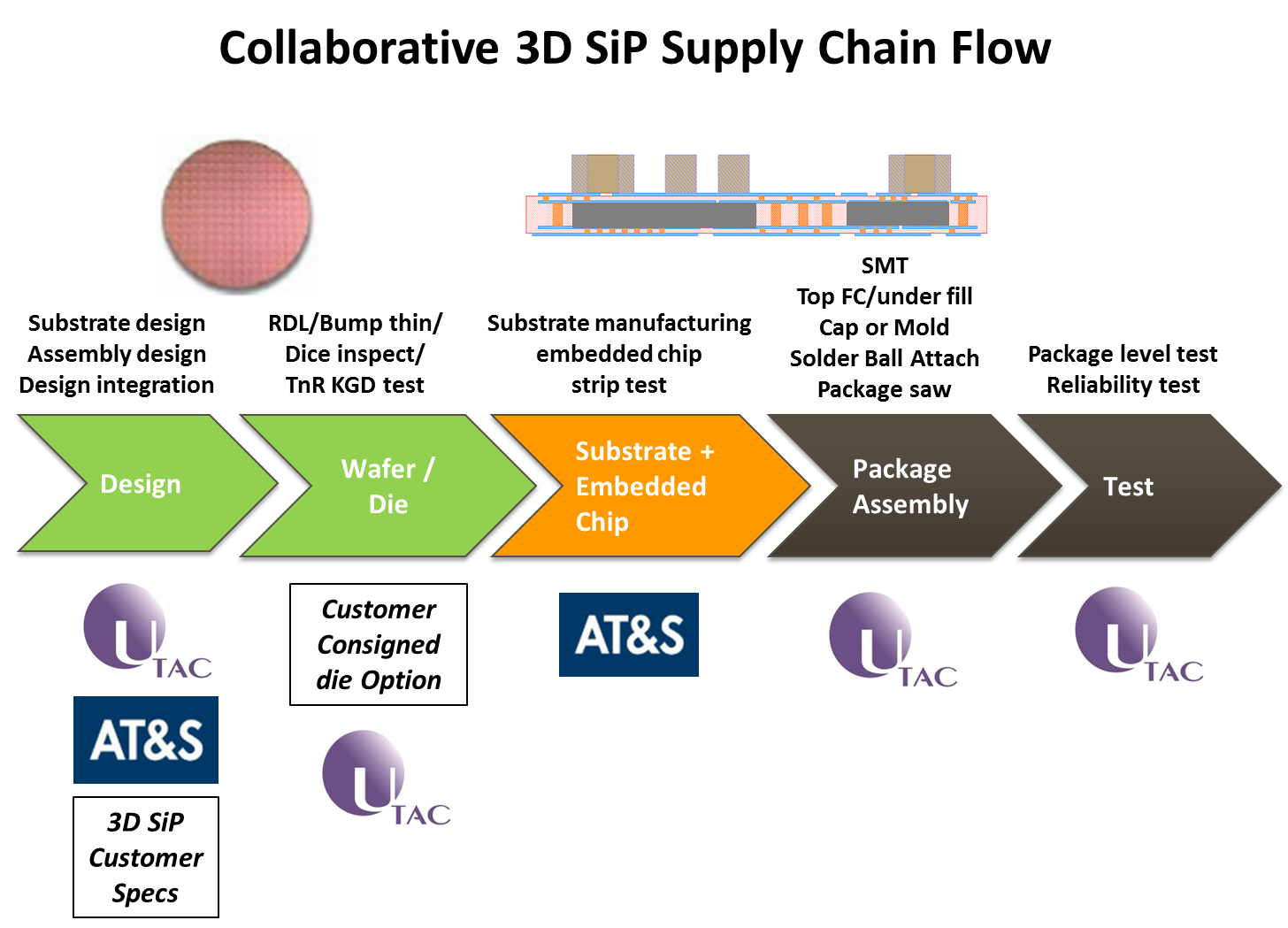
Singapore / Austria, 2. Mai 2016 – UTAC Holdings Ltd (UTAC), one of the leading semiconductor assembly and test services provider in Asia, announced today a joint collaboration with AT&S, one of the global leading manufacturers of high-end printed circuit boards (PCBs) with headquarters in Leoben, Austria, to provide complete turnkey supply chain solutions for three-dimensional system-in-package (“3D SiP”) requirements. The collaboration combines UTAC’s established packaging and test services and AT&S’s industry leading embedded chip in substrate technology. This will offer customers a full turnkey supply chain assembly and test flow for applications that require the heterogeneous integration benefits that the 3D SiP with embedded chip architecture provides.
3D SiP integration benefits include:
- Reduction in package footprint area vs 2D planar SiP technologies
- Improved electrical performance through:
- shorter vertical (plated) interconnects to embedded chips
- 3D architecture enabling closer placement of components
- design flexibility to embed and or surface mount passive components
- Improved thermal performance through:
- lower thermal resistance
- ease of two-sided cooling through embedded chip technology
- EMI / RFI shielding
- shield isolation between digital and RF devices
“UTAC is continuously exploring and developing new technologies with partners in package design and testing to widen our product portfolio. The emerging requirements in power management, timing and RF device applications in particular; demand a new 3D package architecture that is able to handle higher integration and performance at lower costs. We have evaluated various options but none offer the design flexibility, range of benefits and high volume production readiness as AT&S embedded chip technology to deliver 3D SiP solutions,” said Mr. Asif Chowdhury, UTAC Senior Vice President of Product Line & Marketing.
“AT&S has been in production for more than 5 years with our Embedded Component Packaging (ECP®). Until now however, due to the heterogeneous standards, each customer specific supply chain had to be developed and aligned between the various partners. Our collaboration with UTAC provides much needed alignment of roadmaps and design rules for 3D SiP applications. Through the development of this full turnkey supply chain model we are able to address a much broader range of requirements with our embedded chip technology,” said Mr. Michael Lang, AT&S CEO of Advanced Packaging.
Yole Development (Yole) reported that in 2014, AT&S held a 75% share in the embedded die package market which Yole forecasts will grow over 64% annually thru 2020.
Abbreviations:
RDL – Redistribution Layer
TnR – Tape and Reel
KGD – Known Good Die
SMT – Surface Mount Technology
Top FC – Top Flip Chip
About UTAC Holdings Ltd
UTAC Holdings Ltd (UTAC) is a leading independent provider of assembly and test services for a broad range of semiconductor chips and we offer a full range of semiconductor assembly and test services in the following key product categories: analog, mixed-signal and logic, and memory. Our customers are primarily fabless companies, integrated device manufacturers and wafer foundries. UTAC is headquartered in Singapore, with production facilities located in Singapore, Thailand, Taiwan, China, Indonesia and Malaysia, in addition to its global sales network focused on five regions: United States, Japan, China and Taiwan, rest of Asia and Europe, with sales offices located in each of these regions. For more information, please visit www.utacgroup.com
Share news:
Further News
