ECP® technology from AT&S enables evaluation of a fully integrated multilevel power converter on GaN basis

Fraunhofer IAF developed monolithic multilevel voltage converter with high-volt GaN-on-Si technology – test setup with embedding power technology from AT&S demonstrates high performance of the circuit.
Leoben, 25 April 2017 – Fraunhofer IAF has developed a fully integrated monolithic multilevel converter in high-volt AlGaN/GaN-on-Si technology. The integrated inverter circuit is designed for maximum voltages of +/- 400 V and currents of 5 A. The multilevel converter on an area of just 2 × 3 mm² comprises four transistors and six diodes. It provides a perfect solution for compact voltage converter applications. It was possible to demonstrate DC/AC inverter operation for American mains voltage. The circuit exhibits minimal dynamic losses at very high frequencies. The excellent switching performance of the multilevel converter was demonstrated with a test setup on the basis of the ECP® technology from AT&S.
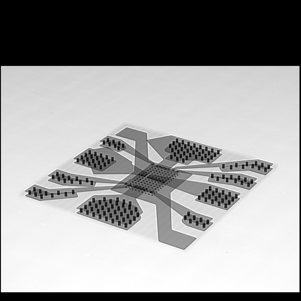
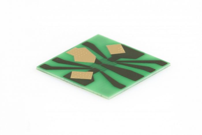
A corresponding test setup is necessary in order to evaluate the chip. The packaging of the die constitutes a key factor in this regard. If lateral components are employed, the source, drain and gate pads are on one side and the back of the die is used for heat dissipation. Since the conventional approach with wirebonds imposed restrictions, the second step of the evaluation saw the ECP® technology from AT&S being used. With this technology, the power components – like the multilevel converter – are embedded into the PCB material and can be connected from both sides. The chips are connected directly via copper-plated microvias. This permits low impedance connections and significantly lower inductances compared with wirebond technology. The rear of the die is also connected by means of copper-plated microvias. This ensures excellent heat dissipation.
“We are highly impressed with the ECP® technology from AT&S and see this mounting technology as opening up entirely new possibilities – particularly also for more complex monolithic integrated GaN power circuits, as used on our multilevel converter chip,” says Richard Reiner, scientist at Fraunhofer IAF. “With a conventional design, we were hardly able to use and/or evaluate the powerful chip.”
“Power electronics constitutes a major field of application and focus for the embedding technology from AT&S,” emphasised Dietmar Drofenik, CEO of the Business Unit Advanced Packaging at AT&S. “Particularly for the use of ‘wide bandgap semiconductor’ materials, such as GaN, the embedding technology makes innovative miniaturised power packages possible for higher efficiencies, enhanced thermal performance and higher power densities. In collaboration with partners, AT&S has for example already implemented various GaN power circuits, which are characterised by excellent switching performance and high efficiency.”
AT&S (Hall 6, Stand 323) and Fraunhofer IAF (Hall 7, Stand 237) are presenting their innovative power solutions at the PCIM 2017 exhibition (16.5. to 18.5.2017) in Nuremberg, Germany.
Share news:
Further News

