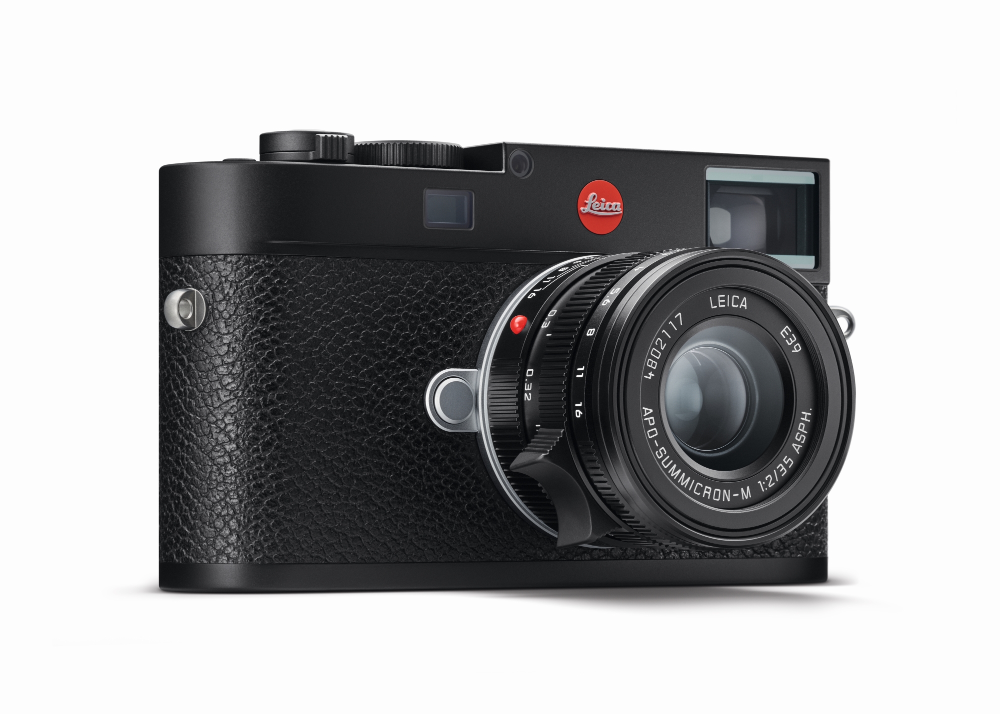
AT&S supplies high-tech components for new Leica M 11

For more than a century, the name Leica has stood for lenses and cameras with the highest quality, first-class workmanship “Made in Germany” and ease of use. Whether photography beginners, ambitious amateur, or professional photographers – they all gladly rely on the high-quality high-tech products from the Leitz Park in Wetzlar (Germany), the corporate headquarters of Leica Camera AG.
With the new Leica M11, the company is once again setting a milestone, combining the unique experience of traditional rangefinder photography with state-of-the-art camera technology. At the heart of the new M generation in the iconic Leica design is a full-frame BSI CMOS sensor with triple resolution technology: raw files in DNG format or JPEGs can be created with a resolution of either 60, 36, or 18 megapixels. Thus, the M11 offers even more flexibility and allows shooting in outstanding image quality.
This is where AT&S, as a development partner of innovative PCB and interconnection technologies, comes into play: A total of twelve different AT&S circuit boards are included in the new M11, including the solutions for integrating the image sensor and image processing. “The trust that a premium manufacturer like Leica places in AT&S products and solutions once again confirms our company’s solution expertise and technological capabilities,” says AT&S CEO Andreas Gerstenmayer.
The printed circuit boards are manufactured both at the Hinterberg site and at the AT&S plant in Korea. The use of special AT&S technologies that allow very compact and flexible electronic interconnection solutions makes it possible for Leica to build digital cameras that offer maximum performance in the smallest possible space while consuming very little energy.
Press contact:
Gerald Reischl, Director Communications & Public Relations
Tel: +43 3842 200 4252; Mobile: +43 664 8859 2452; Send an e-mail
Share news:
Further News
