AT&S offers comprehensive solutions for miniaturisation on all interconnection layers thanks to new toolbox

September 23, 2016 – Constantly increasing system requirements call for ever more efficient solutions with higher power densities and high-speed designs whilst preserving signal integrity. Key growth drivers accompany the digital revolution with increasing networking and growing data volumes and transmission rates. Interconnection technology’s response consists in the further miniaturisation of printed circuit boards and IC substrates in addition to the extensive integration of functions.
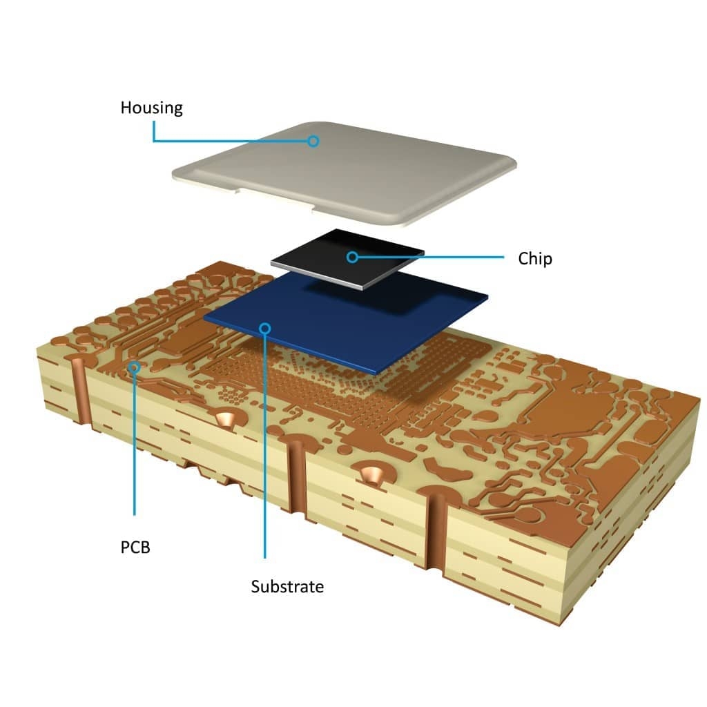
At the same time, the combination of production processes and materials for high-end printed circuit boards with processes and technologies from IC substrate production gives rise to further potential for miniaturisation. AT&S is at the forefront when it comes to using the additional integration of components in substrates and printed circuit boards (embedded component packaging, ECP®) to realise further significant reductions of the measurements in all dimensions. Against this backdrop, the “AT&S Toolbox” provides a vast range of high-end technologies that can be combined with each other for miniaturisation on all interconnection layers.
The “AT&S Toolbox” uses technologies such as insulated metallic substrate (IMS), multilayer, HDI, anylayer, wire-bond-board, flexible PCBs, chip embedding, IC substrates and interposers. For modern SIPs (system in packages), this means that conductor track widths/spacings of 15 µm are possible and significantly less than 10 µm for IC substrates. New high-end systems such as advanced SIPs and SiBs (system in boards) can be largely combined in modular form with all basic technologies. This makes optimised solutions available for customers and the specific applications.
“In future, PCBs will feature ever more advanced packaging solutions. With our AT&S Toolbox, we are perfectly equipped to combine the various technologies in modular and intercompatible concepts,” says Andreas Gerstenmayer, CEO of AT&S and adds “Thanks to the AT&S Toolbox, miniaturisation trends can be implemented efficiently on all layers.”
AT&S is ideally positioned with innovative technologies to supply everything from a single source for the necessary, advancing miniaturisation. IC substrates will also have an important role to play in future. By way of example, the company has already started series production of IC substrates in its new plant in Chongqing, China, where flip-chip ball-grid-array (BGA) substrates are being produced for use with microprocessors. Flip-chip technology constitutes the basis for the packaging and interconnection technology of high-performance semiconductors used in smartphones, tablets and PCs on end-user level and in high-performance graphics workstations, servers and IT infrastructure equipment.
The possibilities that are opened up with the AT&S Toolbox and through the smart combination of various technologies give rise at the same time to new growth potential for the PCB industry. This in turn opens up new markets to manufacturers of high-end PCBs and substrates with embedding technologies. The assembly service sector and the packaging market are particularly worth mentioning here.
Share news:
Further News