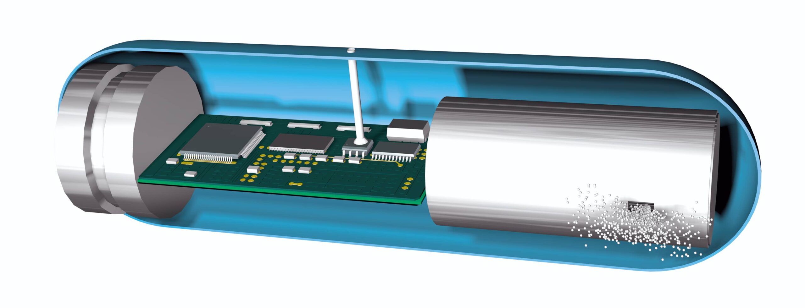
AT&S develops and manufactures miniaturised printed circuit boards for medical technology

Innovative solutions open up new possibilities for hearing aids, pacemakers, prostheses and medical lifestyle products
Leoben, 25 October 2018 – AT&S is addressing the trend towards miniaturisation and digitisation in medical technology as well. At the same time, the systems and components for therapy, diagnosis and patient monitoring are getting smaller, but more powerful. Despite progressive miniaturisation, safety and reliability have top priority. AT&S has developed various technologies that enable the use of its circuit carriers also in innovative applications both on and inside the human body. What is more, the company is one of the few printed circuit board (PCB) manufacturers that is certified to EN ISO 13485, the standard for medical devices.
AT&S’ extensive experience of connection technology in the medical field contributes to making the devices for medical therapy (hearing aids, neurostimulation, pacemakers, prostheses, etc.), for the monitoring of vital signs (blood sugar, blood pressure, ECG) as well as for diagnosis and imaging (MRI, X-ray, ultrasound) even smaller, more powerful and more reliable.
The miniaturisation of medical assemblies requires extremely small interconnect solutions and therefore very small PCB dimensions, with corresponding challenges, e.g. the conductor track widths and distances are currently only 50 μm and are getting smaller and smaller. By way of comparison, the thickness of a human hair measures between 80 μm and 120 μm. The electrical connections of the individual layers are realised using minute ‘stacked vias’. A technological challenge here is the small annular rings around the vias produced using lasers. Thanks to years of experience and high positioning accuracy, designs with 150 μm pad size and 50 μm annular ring are already possible today. The solder resist also has to be positioned very precisely. It is also important to note that the polyimide composite expands or shrinks during processing. This effect has to be minimised or compensated as far as possible. On the one hand, comprehensive expertise and, on the other hand, the use of modern manufacturing techniques and materials are essential to be able to meet all these exacting requirements in the production process in a reproducible and reliable manner.
From the hearing aid to the prosthesis
With sophisticated, reliable technologies, AT&S has for many years been a world-leading PCB supplier for hearing aids, for example. Even modern cochlear implants require a high degree of miniaturisation and use similar technologies. A cochlear implant is an electronic medical device that uses electronic signals to stimulate the defective auditory nerves of the inner ear (cochlea) in order to transmit signals to the brain. For the respective designs different flexible printed circuit boards with usually two to six layers are required. Due to the small installation space, the miniature systems are designed as HDI (High Density Interconnection) or stacked via circuits.
To stabilize the heart rhythm, pacemakers or defibrillators are implanted. Both systems are used for life support and the printed circuit boards used must be very high quality and reliable. For all printed circuit boards used here, therefore, special regulations for process control, which are specified and described in international standards, apply. The materials used must also satisfy specific criteria, which are regularly checked in extensive qualification tests. For many years, AT&S has successfully supplied various customers worldwide with these applications and, thanks to its wealth of experience, can offer added value in the development of sophisticated medical technology solutions.
HDI circuits are used for the control and adjusting unit of prostheses and in the prostheses themselves flexible printed circuit boards are used to implement the dynamic movement can. An important criterion in this regard is that the flexible printed circuit board installed here is constantly being moved with small bending radii. For this purpose, a highly flexible base material with rolled copper is used to ensure the required bending cycles and the low bending radii. Furthermore, the durability of these heavily stressed parts is further increased by special surfaces (carbon print).
Finally, extremely compact interconnection technologies are also being used in wearables and tracking systems for patient monitoring and medical lifestyle applications. The spectrum ranges from mobile medical measuring devices for blood pressure measurement to smart watches and fitness trackers. Again, miniaturisation and reliability is required, but also the lowest possible cost. Against this background, AT&S’ 2.5D technology offers advantages for the implementation of cavities. The defined indents (cavities) in the printed circuit boards can be used to “lower” electronic components such as sensors and even logic components, generally giving the assembled printed circuit board a thinner structure.
Thanks to highly miniaturised PCB technology as a carrier for the corresponding electronics, ‘smart capsules’, which monitor specific body parameters and transmit the relevant data or deliver a controlled dose of medication, are now a reality too.
In addition to the necessary miniaturisation and high quality requirements in medical technology, the development of new biocompatible materials also presents a challenge. AT&S is researching materials that are to be used directly in the body. The objective of this research is twofold: Depending on the field of application, the materials should, on the one hand, be resistant and, on the other hand, have no negative effects on humans themselves and their environment.
AT&S will be presenting its innovative technologies for medical technology at Compamed 2018 from 12 to 15 November in Düsseldorf (Hall 8b, Stand F04-2).
Share news:
Further News
