Sub-5 micrometers: AT&S enters a new dimension with IPCEI
The high-performance microchips used in data centers, which form the basis for AI systems and large-scale data processing, are becoming increasingly complex and fast. In order to reliably and efficiently control and supply power to the billions of transistors in modern processors and graphics processors, the interfaces between the chips and the other components of computers or servers must also be adapted to the shrinking structures. As part of the EU-funded IPCEI on Microelectronics and Communication Technologies project, AT&S is developing a new generation of IC substrates that can establish connections between several high-performance chips and a printed circuit board and allow processors to communicate quickly and efficiently with other components of a computer.
An R&D production line is currently being set up at the new AT&S plant in Leoben, on which the first trials will begin shortly. After years of development work, the employees have thus reached another important milestone. These substrates are not only the first ever to be produced in Europe, but also enter a new technological dimension: The conductor tracks, which will supply microchips with power and data in the future, are only five micrometers wide and can therefore be packed much more densely. This will significantly improve the energy and cost efficiency of the systems.
AT&S is closing in on one of the most important goals that the company has set itself as part of the IPCEI. “The development of the new sub-5 micrometer process shows that our latest IPCEI initiative is already delivering tangible results, which further enhances our competitiveness. But this is just the beginning, we have many more innovations in the pipeline and are already working on making the conductor tracks even smaller,” says Martina Resch, Project Manager R&D Funded Projects at AT&S.
A hair’s breadth is not enough
IC substrates currently available on the market operate with conductor track widths of 8 micrometers, which corresponds to around a tenth of the diameter of a human hair. These structures have to be applied with enormous precision over large areas on the 0.5 by 0.5 meter panels that form the outer layers of a modern IC substrate after cutting. “The semiconductor industry already produces structures thousands of times smaller on microchips, but the processes cannot simply be transferred to substrates. The machines used by microchip manufacturers need small, round silicon wafers that are extremely flat and rigid. We work with large, rectangular panels made of organic material, which are very uneven in comparison and deform due to various influences such as temperature changes,” says Anke Steinberger, Manager R&D Miniaturization at AT&S.
The miniaturization of IC substrates is driven by the requirements of the semiconductor industry, which has to create ever smaller and more densely packed transistors in order to produce processors with higher performance and lower power consumption. In order to handle the increasing number of data and power lines to the transistors and still guarantee efficient connections between several microchips and other system components such as power supply and data storage, the substrates must shrink in tandem with the chips. This is a complex endeavor and requires the development of new processes. It has taken AT&S around five years to acquire the expertise that makes the production of conductor tracks of less 5 micrometers or less possible.
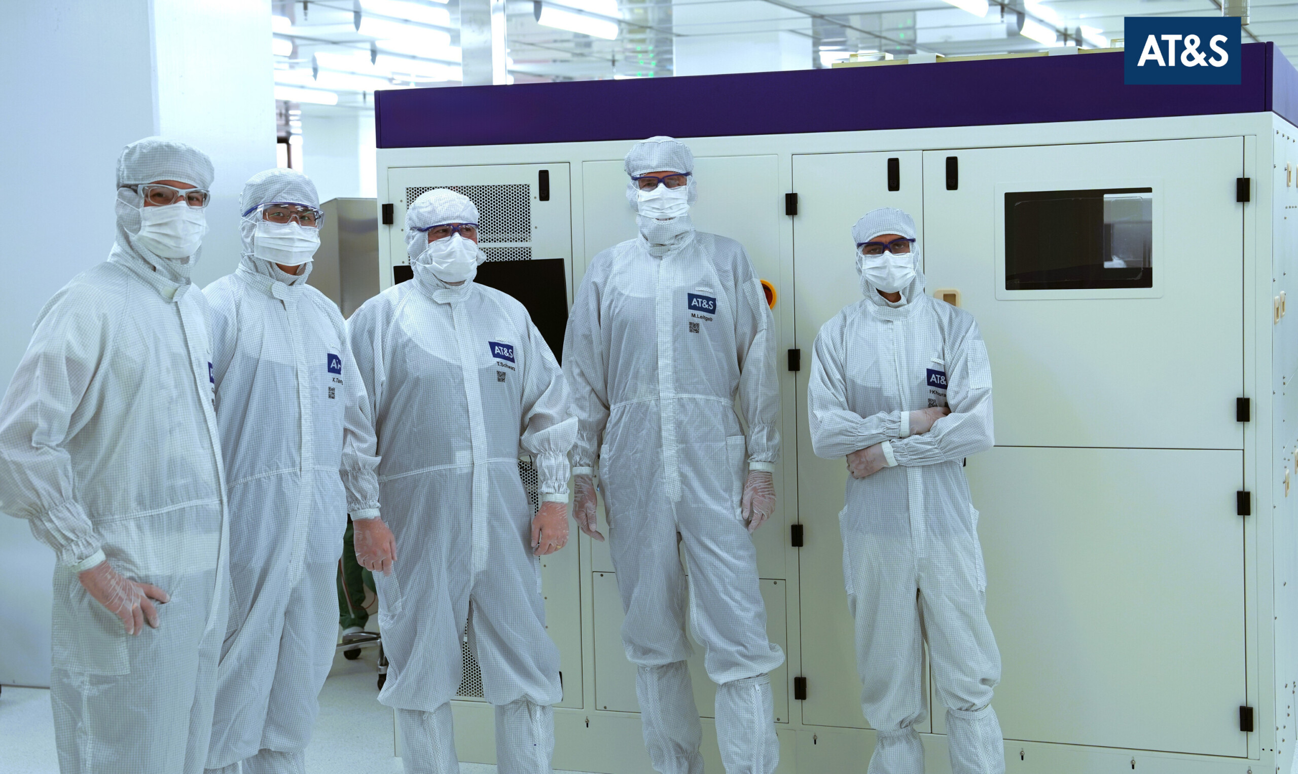
“Our team is currently in the process of setting up and qualifying the new processes in Hinterberg. We have already received initial inquiries from customers and will soon be able to start the first production tests. One of the biggest challenges was to find machines that can support our plans. We use concepts from the semiconductor industry, but we have to adapt them to completely different materials and properties. Fortunately, we found partners with whom we were able to accomplish this,” says Timo Schwarz, who is responsible for the implementation and qualification of the new processes as manager of the R&D line.
No end to miniaturization in sight
The start of the first tests with 5-micrometre tracks is a great success for AT&S, but the miniaturization efforts do not end there. While series production for 5-micrometer substrates is being prepared, technicians are continuing to improve the process. Equipment such as the new exposure machine, which allows our researchers to project the structure of the tiny conductor tracks onto the substrates, supports even smaller circuitry from the outset. “The next step in research will be the implementation of 2-micrometer conductor paths. We will be able to exploit our development line fully in the new plant in the coming years. I have been in the business for 22 years and know from experience that miniaturization never stops. Even if the semiconductor industry talks about physical limits, there are always new ways to develop chips that are more powerful. We have everything we need to make an important contribution to future progress here in Europe,” says Anke Steinberger.

Share post:


